|
Corresponding author: Deepak Bhatia ( dbhatia@rtu.ac.in ) © 2018 Deepak Bhatia, Sandipta Roy, S. Nawaz, R.S. Meena, V.R. Palkar.
This is an open access article distributed under the terms of the Creative Commons Attribution License (CC BY 4.0), which permits unrestricted use, distribution, and reproduction in any medium, provided the original author and source are credited.
Citation:
Bhatia D, Roy S, Nawaz S, Meena RS, Palkar VR (2018) Electrostatic force microscopy analysis of Bi0.7Dy0.3FeO3 thin films prepared by pulsed laser deposition integrated with ZnO films for microelectromechanical systems and memory applications. Modern Electronic Materials 4(2): 77-85. https://doi.org/10.3897/j.moem.4.2.33306
|
Abstract
In this paper, we report the charge trapping phenomena in zinc oxide (n-ZnO) and Bi0.7Dy0.3FeO3 (BDFO)/ZnO thin films deposited on p-type <100> conducting Si substrate. The significant change in contrast above the protrusions of ZnO verifies the possibility of heavy accumulation of injected holes in there. The ZnO and BDFO/ZnO films were characterized by the electrostatic force microscopy (EFM) to understand the phase dependence phenomenon on the bias supporting electron tunnelling. The EFM has an important role in the analysis of electrical transport mechanism characterization and electric charge distribution of local surface in nanoscale devices. It was observed that in BDFO/ZnO, the contrast of EFM images remains constant with the bias switching and that primarily indicates availability of trap sites to host electrons. The change in contrast over the protrusions of ZnO suggests that mobility of the electrical charge carriers may be through the grain boundary. The formation of these hole-trapped sites may be assumed by bond breaking phenomenon.
Keywords
BDFO/ZnO, EFM, multiferroics
1. Introduction
To study the charge trapping phenomena in semiconductor zinc oxide and combination of magnetoelectric multiferroic Bi0.7Dy0.3FeO3(BDFO)/ZnO thin films deposited on p-type Si substrate is an interesting subject. The excellent multifunctional properties of BDFO/ZnO films may be advantageous for a variety of device applications like sensors, energy scavengers, electricity generators, etc [
Zinc oxide (ZnO) is a major contributor in the research field of oxide electronics and may be defined as a future material of choice. This material is suitable for fabrication of the optoelectronic [
The interface between electrode and ferroelectric layer gives rise to complex interfacial physics leads towards degradation of performance of ferroelectric memory elements. The applications of multiferroics are that, they offer the feasibility of best qualities of memory devices with fast low-power electrical write operation, and non-destructive magnetic read operation in a single combination [
1.1 Theory
EFM is used mainly to characterize materials for electrical properties. During the measurements, the tip of standard non-contact EFM system carries out a main scan and an interleave scan on each scanning line. The main scan performs the recording of the surface topographical data in an intermittent contact (tapping) mode [
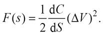 (1)
(1)
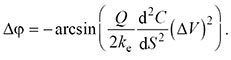
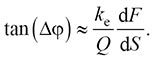
Where ΔV is the potential difference and C is the value of capacitance between the sample and the probe. In the contrast method of EFM-phase measurements technique, the tip is driven mechanically and oscillations are made during the interleave scan. The resonant frequency and phase shift of the tip due to the electrostatic force gradient dF/dS are observed. The resonant frequency (ω) and phase shift (φ) may be defined by the equations 2 and 3 for the small force gradients [
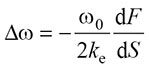 (2)
(2)
and
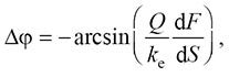 (3)
(3)
where cantilever’s quality factor is «Q» and «ke» is the spring constant. The additional description, practical information and applications of EFM are available in detail and discussed elsewhere [
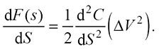 (4)
(4)
Then we have
 (5)
(5)
It is noticed from the equations (4) and (5), the phase and frequency shift is governed by the potential difference ΔV between the tip and the sample surface and finally lateral distribution of d2C/dS2 determines the resolution of the EFM-phase method. This phase shift is always observed to be negative due to the positive value of d2C/dS2. At the same time, owing to the fact that dC/dS is negative the electrostatic forces between the tip and sample surface are attractive.
EFM is also used for mapping of the vertical gradient (S) of the electric field between the sample surface and the tip against the in-plane (X, Y) coordinates. The trapped charges create a field on or below the surface of sample are often adequately large to form a good contrast in an EFM image [
 (6)
(6)
Where Q is quality factor and ke is elastic constant of the cantilever [

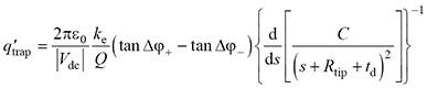
The exerted forces F is the combination of the capacitive and the coulomb force. The trapped charge, qtrap creates the image charges (qi) at the tip and as well as in the semiconductor, where |–q′trap| = 2qtrap/(1 + εsc) . Where εsc is the dielectric constant of ZnO layer. The amount of total tip charge is equal to the sum of the tip bias charge qdc and – q′trap. The surface of tip may be conducted as a sphere-plate capacitor [
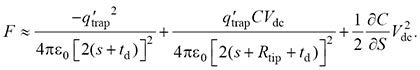 (7)
(7)
Where Rtip is the tip radius and td is the distance between centre of the charge to the sample surface. More expanded terms with qi are excluded for simplicity. Due to the presence of Coulomb force acting between the embedded charge and the image charge, the first term is introduced in the equation (7). Appearance of the second term is from Coulomb forces between the embedded charge and the bias of EFM tip [
2. Experimental Details
A ZnO (99.9%) target of diameter 2 inch was used to deposit ZnO film of 300 nm thickness on RCA (standard Radio Corporation of America) cleaned [
Various techniques were employed for characterization of BDFO/Zno/Si films. The thicknesses of the films were measured by profilometer (Dektak XT). X-ray diffraction (Rigaku, Cu-Kα radiation, λ = 1.5405 Å) was used to determine the phase purity and crystal structure of the film. A Multimode Scanning Probe Microscope (Veeco Digital Instruments make Nanoscope IV) was used to carry out the electric force microscopy of the samples. It was equipped with an optical microscope for area selection. It can zoom-in to examine details up to the limit of the tip’s resolution and high phase sensitivity. Digital image processing and analysis software (Nanoscope 6.2r1) was used to analyze the raw data. The energy-band diagram of the device is shown in Fig.

The electron affinities of ZnO and Si are used as 4.31 and 4.13 eV respectively [28−29], the offsets of conduction-band (ΔEC = χZnO − χSi) and valance-band (ΔEV = ΔEg +ΔEC) are 0.17 and 2.45 eV obtained for n-ZnO/p-Si heterojunction. The movement of holes from Si to ZnO is restricted by the large difference between the valence-band offset and conduction-band offset. Thus, the current transport in the device is dominated by the flow of electrons from the n-ZnO to the p-Si [
3. Results and discussion
XRD Patterns obtained for ZnO and BDFO/ZnO is shown in Fig.
The XRD pattern of ZnO film deposited on Si substrate is single phase and polycrystalline in nature [

 (8)
(8)
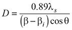
where λs is the wavelength of X-ray Source (1.5405 Å), β and βi (arises from the instrument) are the full width at half maximum (FWHM) of the diffraction peaks and the angle of diffraction is θ.
To determine the grain morphology of BDFO/ZnO and ZnO films, Scanning electron microscopy (SEM) was performed using Raith150Two. It is also used to find the uniformity and the thickness of BDFO films over ZnO films. The SEM images reveal the BDFO coating with granular structure. More details on SEM images are reported in our earlier paper [
A scanning probe microscope (Nanoscope IV Multimode, Veeco Digital Instruments) was used to obtain non-contact mode AFM [Fig.

The sets of AFM images (a–c) of n-type ZnO thin film on 50 nm color scale. Sample scan area is 500 nm and the tip lift-off height is 30 nm, phase sign is decided negative. The sample biases are 0 V, +5V and –5V respectively.
A set of EFM images (a–c) of n-type ZnO is shown in Fig.

The sets of EFM images for ZnO thin film (a–c) on 5° color scale. Sample Scan area is 500 nm and the tip lift-off height is 30 nm. The sample biases are 0 mV, +5V and –5V respectively.
 (9)
(9)
The change in phase with positive bias (+Vdc) to negative bias (–Vdc) is referred as Δφ [

(a) EFM maps are of the phase shift (Distance v/s Phase) graph for Bias voltage 5V (b) Distance v/s Phase graph for Bias voltage –5V.
The amount of the total trapped charges is quantified in the white line circles. Using equation 8, the q′trap is estimated by obtaining averaged phase profile of the set of white line circles positioned at the centre of Fig.
The shift in phases is measured by EFM-phase images and is obtained at different voltage biases between the Au/ZnO/Si film and the conducting probes. A plot of phase shifts within the bias range ±5V at a fixed lift height of 30 nm is shown in Fig.

y = A + Bx + Cx2.
Where, A (V) is the bias voltage in mV, B (φ) is the phase in degree and C is independent variable and phase difference (Δφ) is given by equation (5).
As described by equation (5) and observed in Fig.
The sets of AFM images of BDFO/ZnO thin films on 50 nm color scale and EFM images on 5o color scale are shown in Fig.

The sets of AFM images (a–c) of BDFO/ZnO thin films on 50 nm color scale and EFM images (d–f) on 5° color scale. Sample scan area is 500 nm and tip lift off height is 30 nm. The sample biases are 0 V, +5V and –5V respectively.

The effect of positive charges on total conductance is verified by Conductive AFM (c-AFM) with 8 V for ZnO films will be reported in another article. It is anticipated such an embedded hole in ZnO to increase the amount of total current with bias voltage by lowering the practical tunnelling barrier [
4. Conclusion
The charge trapping phenomena in the n-ZnO and BDFO/ZnO films were observed microscopically. It was concluded that in BDFO/ZnO, the contrast of EFM images remains constant with the bias switching and that indicates the trap sites are primarily available to host electrons. The change in contrast over the protrusions of ZnO shows that injected holes are heavily accumulated and easy mechanism of mobility of the electrical charge carriers may be through the grain boundary. The formation of these hole-trapped sites may be assumed bond breaking phenomenon. These trapped holes decrease the height of potential barrier, resulting in flow of additional amount of current. The process of EFM-phase measurements yields significant information contents about the surface of a sample. There is a possibility to excerpt the surface potential of sample, work function, capacitance and even comparison of the surface resistivity with appreciable resolution from the analysed phase data. The phase–voltage relationship was performed on a ZnO sample surface by fitting the obtained EFM-phase data using a parabolic method in the potential range of −5 to +5 V. Thus phase data may be converted to voltage data, and enables the use of EFM phase mode for measuring the surface potential of an unknown region. The validity of this procedure is both for semiconductor and metallic surfaces. Finally, a good understanding has been found about the electrical charge transport on ZnO and BDFO/ZnO thin films from these results. It may provide its relevant improvements for application as a piezoelectric layer and memory element in MEMS energy scavengers, transparent electrodes in some photovoltaic devices and on chip transformers.
Acknowledgement
The authors wish to acknowledge the partial funding (Grant No. 08DIT006 and 13DIT006) received from the Department of Information Technology, Government of India, through the Centre of Excellence in Nanoelectronics, IIT Bombay under INUP. The authors also acknowledge to Department of Physics and Department of Material Science, IIT Bombay and Rajasthan Technical University, Kota for experimental help.
References
- 1 Mandal M., Chatterjee S., Palkar V.R Multifunctional behavior of ZnO supported Bi1-xDyxFeO3 nanorods. J. Appl. Phys. 2011; 110: 054313. https://doi.org/10.1063/1.3636274
- 2 Kim Y.H., Kim J.S., Kim W.M., Seong T.-Y., Lee J., Müller-Meskamp L., Leo K. Realizing the potential of ZnO with alternative non-metallic Co-dopants as electrode materials for small molecule optoelectronic devices. Adv. Funct. Mater. 2013; 23(29): 3645–3652. https://doi.org/10.1002/adfm.201202799
- 3 Dodds J.S., Meyers F.N., Loh K.J. Piezoelectric characterization of PVDF-TrFE thin films enhanced with ZnO nanoparticles. IEEE Sens. J. 2012; 12(6); 1889–1890. https://doi.org/10.1109/JSEN.2011.2182043
- 4 Prepelita P., Medianu R., Garoi F., Stefan N., Iacomi F. On the structural and electrical characteristics of zinc oxide thin films. Thin Solid Films. 2010; 518(16): 4615–4618. https://doi.org/10.1016/j.tsf.2009.12.044
- 5 de la L Olvera M., Maldonado A., Asomoza R., Tirado-Guerra S. Characteristics of transparent and conductive undoped ZnO thin films obtained by chemical spray using zinc pentanedionate. Thin Solid Films. 2002; 411(2): 198–202. https://doi.org/10.1016/S0040-6090(02)00248-1
- 6 Pearton S.J., Norton D.P., Heo Y.W., Tien L.C., Ivill M.P., Li Y., Kang B.S., Ren F., Kelly J., Hebard A.F. ZnO spintronics and nanowire devices. J. Electron. Mater. 2006; 35(5): 862–868.https://doi.org/10.1007/BF02692541
- 7 Nagata T., Oh S., Yamashita Y., Yoshikawa H., Ikeno N., Kobayashi K., Chikyow T., Wakayama Y. Photoelectron spectroscopic study of band alignment of polymer/ZnO photovoltaic device structure. Appl. Phys. Lett. 2013; 102(4); 043302–043304. https://doi.org/10.1063/1.4790298
- 8 Maragliano C., Stefancich M., Rampino S., Colace L. Realistic simulation of polycrystalline CIGS absorbers and experimental verification. MRS Online Proceedings Library. 2013; 1493: 153–160. https://doi.org/10.1557/opl.2013.401
- 9 Repins I., Contreras M., Romero M., Yan Y., Metzger W., Li J., Johnston S., Egaas B., DeHart C., Scharf J., McCandless B.E., Noufi R. Characterization of 19.9%-efficient CIGS absorbers. 33rd IEEE Photovoltaic Specialists Conference. 2008; 235–239. https://doi.org/10.1109/PVSC.2008.4922628
- 10 Maragliano C., Colace L., Chiesa M., Rampino S., Stefancich M. Three-dimensional Cu(InGa)Se2 photovoltaic cells simulations: optimization for limited-range wavelength applications. IEEE J. Photovoltaics. 2013; 3(3): 1106–1112. https://doi.org/10.1109/JPHOTOV.2013.2258191
- 11 Lilliu S., Agostinelli T., Pires E., Hampton M., Nelson J., Macdonald J.E. Dynamics of crystallization and disorder during annealing of P3HT/ PCBM bulk heterojunctions. Macromolecules. 2011; 44(8): 2725–2734. https://doi.org/10.1021/ma102817z
- 12 Krebs F.C. Fabrication and processing of polymer solar cells: A review of printing and coating techniques. Sol. Energy Mater. Sol. Cells. 2009; 93(4): 394–412. https://doi.org/10.1016/j.solmat.2008.10.004
- 13 Scott J.F. Data storage: Multiferroic memories. Nat. Mater. 2007; 6: 256–257. https://doi.org/10.1038/nmat1868
- 14 He C., Ma Z.-J., Sun B.Z., Sa R.J., Wu K. The electronic, optical and ferroelectric properties of BiFeO3 during polarization reversal: A first principle study. J. Alloy Comp. 2015; 623 393–400. https://doi.org/10.1016/j.jallcom.2014.11.062
- 15 Peng Lin, Simin Cui, Xierong Zeng, Haitao Huang, Shanming Ke. Giant dielectric response and enhanced thermal stability of multiferroic BiFeO3. J. Alloy Comp. 2014; 600: 118–124. https://doi.org/10.1016/j.jallcom.2014.02.128
- 16 Sunil Chauhan, Manoj Kumar, Sandeep Chhoker, Katyal S.C. A comparative study on structural, vibrational, dielectric and magnetic properties of microcrystalline BiFeO3, nanocrystalline BiFeO3 and core-shell structured BiFeO3@SiO2 nanoparticles. J. Alloy Comp. 2016; 666: 454–467. https://doi.org/10.1016/j.jallcom.2016.01.116
- 17 Chia-Shiu Yeh, Jenn-Ming Wu. Characterization of Pt/multiferroic BiFeO3/(Ba,Sr)TiO3/Si stacks for nonvolatile memory applications Appl. Phys. Lett. 2008; 93(15): 154101. https://doi.org/10.1063/1.3001800
- 18 Palkar V.R., Prashanthi K. Observation of magnetoelectric coupling in Bi0.7Dy0.3FeO3 thin films at room temperature. Appl. Phys. Lett. 2008; 93(13): 132906. https://doi.org/10.1063/1.2994692
- 19 Prashanthi K., Chalke B.A., Bapat R.D., Purandare S.C., Palkar V.R. Multiferroic Bi0.7Dy0.3FeO3 thin films directly integrated on Si for integrated circuit compatible devices. Thin Solid Films. 2010; 518(20): 5866–5870. https://doi.org/10.1016/j.tsf.2010.05.060
- 20 Fain (Jr.) S.C., Barry K.A., Bush M.G., Pittenger B., Louie R.N. Measuring average tip-sample forces in intermittent-contact (tapping) force microscopy in air. Appl. Phys. Lett. 2000; 76(7): 930–932. https://doi.org/10.1063/1.125633
- 21 Lei C.H., Das A., Elliott M., Macdonald J.E. Quantitative electrostatic force microscopy-phase measurements. Nanotechnology. 2004; 15(5): 627–634. https://doi.org/10.1088/0957-4484/15/5/038
- 22 Sarid D. Scanning force microscopy: with applications to electric. Magnetic and Atomic Forces. Oxford: Oxford University, 1994.
- 23 Bonnell D. Scanning probe microscopy and spectroscopy: theory, techniques and applications. New York: Wiley-VCH, 2000.
- 24 Serry F.M., Kjoller K., Thornton J.T., Tench R.J., Cook D. Electric force microscopy surface potential imaging and surface electric modifications with AFM. Bruker, 2010. URL: http://nano.boisestate.edu/wp-content/uploads/2010/12/Bruker-AN-27-EFM-Surface-Potential.pdf
- 25 Kim J.-H., Noh H., Khim Z.G, Jeon K.S., Park Y.J., Yoo H., Choi E., Om J. Electrostatic force microscopy study about the hole trap in thin nitride/oxide/semiconductor structure. Appl. Phys. Lett. 2008; 92(13): 132901. https://doi.org/10.1063/1.2904646
- 26 Kang C.J., Buh G.H., Lee S., Kim C.K., Mang K.M., Im C., Kuk Y. Charge trap dynamics in a SiO2 layer on Si by scanning capacitance microscopy. Appl. Phys. Lett. 1999; 74(13): 1815. https://doi.org/10.1063/1.123095
- 27 Wangsness R.K. Electromagnetic field. New York: Wiley, 1979.
- 28 Majumdar S., Banerji P. Temperature dependent electrical transport in p-ZnO/n-Si heterojunction formed by pulsed laser deposition. J. Appl. Phys. 2009; 105(4): 043704. https://doi.org/10.1063/1.3078806
- 29 Bhatia D., Roy S., Nawaz S., Meena R.S., Palkar V.R. Room temperature electrical properties of Bi0.7Dy0.3FeO3 thin films deposited by PLD on ZnO films for potential applications. Microelectronic Engineering. 2016; 163: 60–66. https://doi.org/10.1016/j.mee.2016.06.003
- 30 Somvanshi D., Jit S. Analysis of temperature-dependent electrical characteristics of n-ZnO nanowires (NWs)/p-Si heterojunction diodes. IEEE Transactions on Nanotechnology. 2014; 13(1): 62–69. https://doi.org/10.1109/TNANO.2013.2290553
- 31 Lee J.D., Park C.Y., Kim H.S., Lee J.J., Choo Y.G. A study of conduction of ZnO film/p-Si heterojunction fabricated by photo induced electro deposition under illumination. J. Phys. D: Appl. Phys. 2010; 43(36): 365403-1–365403-6. https://doi.org/10.1088/0022-3727/43/36/365403
- 32 Qian F.Z., Jiang J.S., Guo S.Z., Jiang D.M., Zhang W.G. Multiferroic properties of Bi1-xDyxFeO3 nanoparticles. J. Appl. Phys. 2009; 106(8): 084312 https://doi.org/10.1063/1.3245390
- 33 Tao Xu, Guoying Wu, Guobing Zhang, Yilong Hao. The compatibility of ZnO film with micromachining process. Sensors and Actuators A: Physical. 2003; 104(1): 61–67. https://doi.org/10.1016/S0924-4247(02)00484-3
- 34 Yao Wang, Ce-Wen Nan. Integration of BiFeO3 thin films on Si wafer via a simple sol-gel method. Thin Solid Films. 2009; 517(15): 4484–4487. https://doi.org/10.1016/j.tsf.2009.02.142
- 35 Middleton A.A., Wingreen N.S. Collective transport in arrays of small metallic dots. Phys. Rev. Lett. 1993; 71(19): 3198. https://doi.org/10.1103/PhysRevLett.71.3198
- 36 Bresse J.-F. Contact potential difference of Au and GaInAs by electrostatic force microscopy. Microchimica Acta. 2000; 132(2–4): 449–455. https://doi.org/10.1007/s006040050093
- 37 Sze S.M. Physics of semiconductor devices. Chichester: Wiley, 1981.
- 38 Rousier R., Vairac P., Cretin B. Measurement of the contact potential difference with an electrostatic force microscope. Eur. J. Phys. 2001; 22(6): 657–662. https://doi.org/10.1088/0143-0807/22/6/311
- 39 Seko A., Watanabe Y., Kondo H., Sakai A., Zaima S., Yasuda Y. Analysis of local breakdown process in stressed gate SiO2 films by conductive atomic force microscopy. Jpn. J. Appl. Phys. 2005; 10(44 Pt 1): 7582–7587. https://doi.org/10.1143/JJAP.44.7582