Research Article |
|
Corresponding author: Alexander K. Fedotov ( fedotov@bsu.by ) © 2021 Andrei A. Kharchenko, Julia A. Fedotova, Valeryia Yu. Slabukho, Alexander K. Fedotov, Alexey V. Pashkevich, Ivan A Svito, Maxim V. Bushinsky.
This is an open access article distributed under the terms of the Creative Commons Attribution License (CC BY 4.0), which permits unrestricted use, distribution, and reproduction in any medium, provided the original author and source are credited.
Citation:
Kharchenko AA, Fedotova JuA, Slabukho VYu, Fedotov AK, Pashkevich AV, Svito IA, Bushinsky MV (2021) Electrical and galvanomagnetic properties of black phosphorus single crystals. Modern Electronic Materials 7(4): 127-139. https://doi.org/10.3897/j.moem.7.4.78587
|
Abstract
Black phosphorus (b-P) single crystals having the n-type electrical conductivity produced in a high pressure set-up (~1 GPa) with six diamond anvils at 800 °C for 12 h have been studied. The electrical conductivity σ(Т,В) and the Hall constant Rh(Т,В) have been analyzed within one-band and two-band models as functions of temperature in the 2 < Т < 300 K range and magnetic field in the 0 < В < 8 T range. Fitting of the experimental σ(Т,В) and Rh(Т,В) curves suggests the following key properties of the crystals: (1) intrinsic conductivity type, (2) approximately equal electron and hole concentrations and mobilities, (3) anisotropic behavior of electron and hole conductivities, concentrations and mobilities and (4) combination of negative and positive contributions to magnetoresistance (magnetoresistive effect, MR). In a zero magnetic field the anisotropy coefficient α = [σа (Т) – σс (Т)]/σс (Т) below 50–70 K is positive whereas above 220 K its sign changes to negative due to a specific combination of the temperature dependences of carrier concentration and mobility. It has been shown that the negative sign of relative MR (negative magnetoresistive effect) dominates at T < 25 K and B < 6 T and is presumably caused by the effects of strong localization resulting from structural disorder. The positive MR sign (positive magnetoresistive effect) is associated with the Lorentz mechanism of carrier movement and exhibits itself above 25 K in 6–8 T magnetic fields.
Keywords
black phosphorus, conductivity anisotropy, magnetoresistance, carrier transport, two-band model.
1. Introduction
Black phosphorus (b-P) is one of the most atmospheric-pressure stable allotropic phosphorus modifications pertaining to the series of materials having a new-type layered 2D structure [
As can be seen from Fig.
Studies of bulk black phosphorus started after P.U. Bridgman first synthesized it in 1914 at high pressures and temperatures [
Despite the obvious success in phosphorene research there are still a number of pending questions in the understanding and explanation of the properties (primarily, electric ones) of bulk b-P crystals. Below is a brief overview of literary data on the electrical properties of bulk polycrystalline and single crystalline black phosphorus obtained using various methods.
Works dealing with the properties of black phosphorus can be arbitrarily divided in 2 groups: in the period from 1914 to approx. 1990 [2, 6, 20–24] and after 2014 [1, 3–5, 7–19, 25–33] when interest to b-P arose again due to the production of b-P single crystals having a higher structural perfection. There are multiple literary data on the electrical resistivity and Hall effect of bulk b-P single crystals over a wide range of temperatures and magnetic fields [
As noted above, earlier data [20, 24, 25, 27, 29–33] suggest (see for example Fig.
As noted earlier [
The behavior of anisotropic semiconductors and semimetals (especially those having nontrivial carrier dispersion laws) in magnetic fields plays a key role in the understanding of their carrier transport mechanisms. The first data on the magnetoresistive effect in b-P crystals were reported in the earliest works on the topic [
The PMR to NMR transition [
1. With an increase in the magnetic field the longitudinal contribution to the resistivity tensor ρхх (B) does not undergo saturation in the PMR region whereas in the NMR region its saturation occurs.
2. The Hall resistivity ρхх (B) grows linearly with an increase in the magnetic field at 3 and 300 K but exhibits a nonlinear behavior in the entire range of intermediate temperatures, i.e., 20–200 K.
The former specific feature of the ρхх (B) behavior under impact of magnetic field results in necessity to describe it by two models, i.e., the classical resistor array model (caused by disorder) and the magnetic polaron model (due to the high ohmicity of the crystal) [
The latter specific feature of the ρхх (B) behavior in a magnetic field is accounted for on the basis of two-band conductivity models involving two types of carriers.
Analysis of literary data on carrier transport in bulk black phosphorus crystals discovers a wide range of models based on which black phosphorus electrical properties are described. It should be noted that there are scarce data on the influence of b-P crystal growth technology (primarily, synthesis process pressure, temperature duration and atmosphere), defect state (single crystal, polycrystal, type and quantity of defects, deformation etc.) and measurement mode (number of heating/cooling cycles, storage time and atmosphere) on the temperature dependences of electrical resistivity, magnetoresistive effect, Hall effect, Seebeck effect and other properties of the material. For this reason a number of questions as to the nature of the electrical properties formation in black phosphorus bulk crystals have not been clarified as yet.
Below we present data on the temperature dependences of the electrical conductivity, magnetoresistance and Hall effect for several b-P bulk single crystals made by 2D Semiconductors, USA.

(a) Schematic of rifled layered structure, (b) layer top view and (c) layer fragment in b-P lattice [4, 5].


2. Experimental
The single crystals were synthesized in a high pressure plant (~1 Gpa) with six diamond anvils at 800 °C for 12 h following a technology similar to a earlier described one [
Standard measurements of the electrical resistivity R (T,В) and the Hall constant Rh(T,В) of the black phosphorus single crystals were carried out in the 2 < T < 300 K temperature range at 0 ≤ B < 8 T magnetic fields. The test specimens were rectangular, their longer sides (and hence the current vector directions) being parallel to the a crystallographic axis (Specimen 1) or the c axis (Specimen 2) and the B vector being always perpendicular to the ac plane, i.e., it was along the b axis. The R (T,В) and Rh(T,В) dependences were recorded in a cryogen-free measurement system of Cryogenics Ltd., UK, on the basis of a closed-cycle refrigerator. The current through the specimens during the measurements was set and measured with a Keithley 6430 unit which allows measuring electrical resistance in the 100 mΩ to 10 GΩ range accurate to within 0.1%. The temperature of the specimens was controlled with LakeShore thermodiodes calibrated accurate to 0.0005 K and having a reproducibility of 0.001 K. The temperature was stabilized and measured with a LakeShore 331 controller. The measurement accuracy of the conductivity σ and the Hall constant Rh was not worse than 5%, the error being mostly determined by the measurement error in specimen dimensions, electric contact width and contact spacing. Room temperature Hall effect and Seebeck effect sign measurements showed that the test single crystals had the n type conductivity. The stability of the Hall effect sign testified to the predominantly electron conductivity over the whole test temperature range. The quality of the contacts for all the specimens was checked by preliminary measurement of IVs at T = 300 K which proved to be linear at currents of below 1 mA.
3. Results and discussion
Figure
The tests showed that the b-P specimens exhibit a strong conductivity anisotropy showing itself primarily in the difference between the behavior of σа (Т) and σс (Т) in the measuring temperature range with the current vector being always oriented along the a or c axes, respectively. It can be seen from Fig.
The test showed that Rh(В) in fields stronger than 1 T at any temperatures is almost insensitive to magnetic field magnitude. Figure
To correctly estimate the carrier concentrations and adequately describe the carrier transport mechanisms in single crystal b-P Specimens 1 and 2 we additionally studied the relative magnetoresistance MR (В,Т) = [R (B) – R (0)]/R (0) as a function of magnetic field and temperature (Fig.
Analysis of the curves showed that in magnetic fields with magnitudes greater than Bm the absolute values of NMR effect and in the whole range of PMR contribution, the MR (В) curves are proportional to B2 suggesting its Lorentz nature. One should note a number of specific features inherent to the behavior of this contribution with a change in temperature. At 10 K the magnetoresistive effect (even after subtraction of the NMR contribution) is the smallest (almost zero) as compared with its values at higher temperatures although there are indications [
As shown above the experiments revealed a strong anisotropy of the electrical conductivity and magnetoresistance, including a change in the sign of the anisotropy coefficient α = [σа (Т) –σс (Т)]/σс (Т). This anisotropy shows itself not only as the dependence of the conductivity and MR on current vector orientation relative to the crystallographic axes of b-P single crystals but also as a change in the course of the σ(Т) (semiconducting- or metallic-like) curves and the magnetoresistive effect as a function of magnetic field and temperature MR (В,Т) (NMR or PMR). As follows from the brief literature review presented above the main features of the σ(Т), Rh(В,Т) and MR (В,Т) curves for b-P bulk crystals are explained in different sources within four most widely used approaches.
1. Movement of one type of carriers (holes) in intrinsic b-P crystals (single-band model) [
2. Movement of two different-sign carriers with different effective masses in two bands [
3. Movement of carriers in large-scale potential pattern relief causing the so-called mobility fluctuations [
4. Movement of carriers under strong localization conditions (hopping conductivity of carriers or polarons) [
We will now justify the criteria of choosing one of the above listed approaches that we will use hereinafter for analyzing the experimental σ(Т), Rh(В,Т) and MR (В,Т) dependences and discussing the measurement results.
The use of the single-band model in the former case for analysis of the movement of one type carriers is most likely incorrect for the following reasons. First, this model is only applicable to undoped b-P which is an intrinsic semiconductor and should have predominantly hole conductivity type since the effective mass of holes is lower than that of electrons [
The model allowing for carrier movement in the large-scale potential relief region is typically used for analysis of Hall mobility in heavily inhomogeneous semiconductors containing large-scaled structural defects. In b-P crystals these defects can be grain boundaries (in polycrystals), dislocations, interlayer cracks (caused by the extremely high brittleness of these crystals), stacking faults (violation of the layering rule of phosphorus atoms) as well as point defect clusters. The presence of large-scale potential relief in inhomogeneous semiconductor crystals shows itself at low temperatures when and if the temperature dependence of μh(Т) in double logarithmic coordinates is linear and has extra large positive slopes (the exponent values k >> 3/2) [
Attempts to describe carrier movement under strong localization conditions showing itself as hopping or polaron conductivity at temperatures below 40–50 K also failed because low-temperature σ(Т) curves in Mott’s coordinates [
Analysis of the possibility to use the four abovementioned most widely used approaches to the description of the σ(Т), Rh(В,Т) and MR (В,Т) dependences showed that correct description of the magnetoresistive properties of b-P requires the two-band model be used. Note also that when discussing the properties of b-P single crystals we ruled out Drude’s theory of quantum corrections to the conductivity due to a carriers phase breaking under weak localization conditions which was formerly observed only in single- or multilayered specimens of splitted phosphorene, graphene and transition metal chalcogenides [

Relative magnetoresistance MR (В,Т) for black phosphorus specimens (a) 1 and (b) 2 as a function of magnetic field B at different temperatures T, K: (1) 2; (2) 5; (3) 10; (4) 25; (5) 50; (6) 100; (7) 150; (8) 200; (9) 250; (10) 275; (11) 300.

(a) Hall mobility vs temperature dependences µh(T) in linear coordinates and (b) Hall concentration vs temperature dependences nо(T) in double logarithmic coordinates for Specimens (1) 1 and (2) 2. Inset: µh(Т) dependences in double logarithmic coordinates.
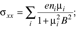
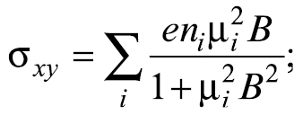
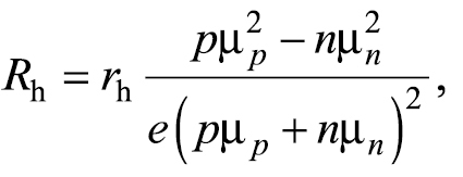
For a quantitative evaluation of the parameters describing the conductivity and galvanomagnetic properties of b-P single crystal Specimens 1 and 2 on the basis of the two-band model [
 (1a)
(1a)
 (1b)
(1b)
 (1c)
(1c)
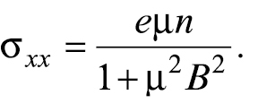
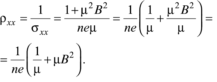
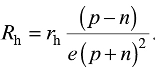
where μi, ni are the mobility and concentration of i-th type carriers (i = p, n), respectively, B is the magnetic field induction in which the specimen is located, e is the electron charge and rh is the Hall factor. Since the Hall coefficient does not depend on magnetic field at В > 1 T then assuming electron and hole mobilities to be equal (μi = μ) we can rewrite Eqs. (1a)–(1c) as follows:
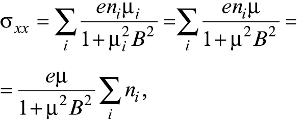 (2)
(2)
where
 (3)
(3)
is the sum of the carrier concentrations. Then Eq. (1a) reduces to the following relation:
 (4)
(4)
Introducing the relationship
 (5)
(5)
we obtain the formula for relative magnetoresistance tensor:
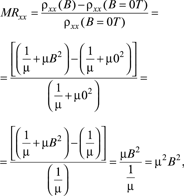 (6)
(6)
where μ0 is the mobility at B = 0. This implies the equality
 (7)
(7)
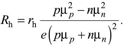
For the two carrier types having different signs (electrons and holes) and mobilities in classically weak magnetic fields μ2В2 << 1 for which rh depends on the scattering mechanism [
 (8)
(8)
whereas for μp = μe = μ it transforms as follows:
 (9)
(9)
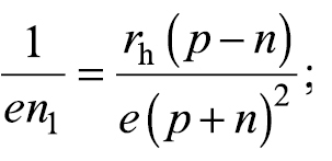
Therefore, the experimental value 1/eRh will be related to the actual carrier concentrations (n and p) through the following formula:
 (10)
(10)
In this case the conductivities for equal electron and hole mobilities (μp = μe = μ) and for co-existence of two different-sign carrier types will be as follows:
σ = σh + σe = enμ + epμ = eμ (n + p) = eμn2, (11a)
σ = σh + σe = enμe + epμh, (11b)
whence
n 2 = (n + p). (12)
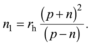
Therefore, the n1 parameter in Eq. (10) can be obtained by measuring the Hall coefficient (1/eRh), the n2 parameter can be borrowed from the conductivity formula (Eq. (11a)) and the mobility can be calculated using Eq. (6) for the MRxx parameter:
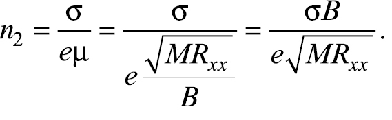 (13)
(13)
Simple transformations of Eqs. (1) and (12) yield the following set of equations for n and p calculation:
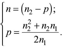 (14)
(14)
The relationships obtained above (Method 1) will be hereinafter used for the calculations of carrier concentrations and mobilities (provided the latter are equal).
To estimate these parameters in the assumption of the electrical neutrality condition (if the b-P crystals are accepted to be intrinsic semiconductors) we will consider the electron and hole concentrations to be equal:
n = p. (15)
Then the conductivity, the Hall constant and the magnetoresistance will be respectively described by the following relationships [
σ = σh + σe = enμe + epμh = eN (μe + μh); (16a)
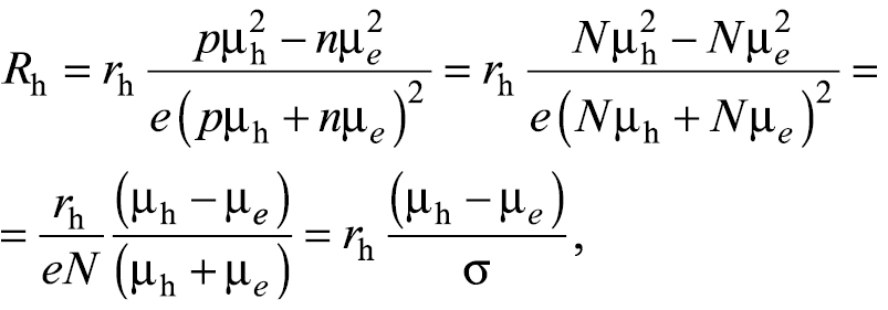 (16b)
(16b)
 (16c)
(16c)
Introducing the notations
 (17a)
(17a)
 (17b)
(17b)
 (17c)
(17c)
we obtain the following set of equations for the calculation of mobilities:
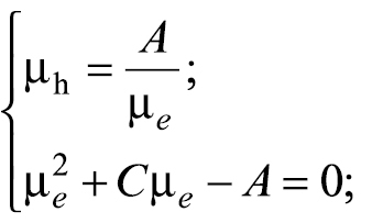
D = C2 – 4A,
which has two solutions:
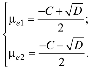 (18)
(18)
Calculations using Eqs. (15)–(18) are the principle of Method 2.
We will now estimate some parameters of the test b-P single crystal specimens using Methods 1 and 2 for the fitting of the galvanomagnetic properties as described above. It should be noted that for calculations based on either of the Methods using the experimentally observed magnetoresistive effect MR (T,B) at temperatures below 25 K we took into account the NMR contribution to the magnetoresistive effect in the region of a magnetic field by subtracting its maximum absolute value at В = Bm (see insets in Fig.
Results of fitting using both Methods described above for derivation of the electron and hole concentration and mobility temperature dependences yield close values, see Figs

(a) Electron and hole concentrations (n = p) vs temperature and (b) electron-to-hole concentration ratio (n/p) for Specimens (1) 1 and (2) 2. Inset: same functions in double logarithmic coordinates.

(a) Electron and hole mobilities µ(T) vs temperature and (b) electron-to-hole mobility ratio (µn/µр) for Specimens (1) 1 and (2) 2. Inset: mobility vs temperature in double logarithmic coordinates.
| Specimen | Concentration (1019 m-3) | Mobility (m2/(V⋅s)) | ||||
| n | p | n = p | μn | μp | μp = μn = μ | |
| Method 1 | Method 2 | Method 2 | Method 1 | |||
| 1 | 7.878 | 7.860 | 7.869 | 0.02212 | 0.02210 | 0.02211 |
| 2 | 3.328 | 3.332 | 3.330 | 0.02148 | 0.02147 | 0.02147 |
Before discussing the dependences shown in Figs
Analysis of the dependences shown in Fig.
The behavior of the n (Т) and p (T) dependences described above suggests that the experimental b-P single crystals are intrinsic semiconductors with predominantly electron conductivity type.
As can be seen from Fig.
There is an obvious correlation between the curve behavior shown in Fig.
On the other hand, since the carrier concentration for Specimen 1 shown in Fig.
It follows from the above that the conductivity anisotropy is mainly determined by the carrier concentration anisotropy. Since the carrier concentration and mobility in Specimen 1 see a saturation plateau at high temperatures whereas the carrier concentration in Specimen 2 always grows with temperature, the sign of the conductivity anisotropy in Specimen 2 changes. Thus the correlation between the temperature behavior of the conductivity shown in Fig.
We will now compare the presence and behavior of the NMR effect in the test b-P specimens at low temperatures (Fig.
The NMR effect is often observed in strongly disordered semiconductors (i.e., under strong localization conditions) when hopping electron transport over localized states occurs [
4. Conclusion
Study of the galvanomagnetic properties of black phosphorus (n-P) single crystals showed that these crystals are intrinsic semiconductors with two carrier types (electrons and holes) having almost equal concentrations and mobilities. The temperature dependence of the electrical conductivity σ(Т) is determined by the orientation of the current vector relative to the a and c crystallographic axes and depends primarily on the carrier concentration anisotropy. At below 50–70 K the anisotropy coefficient α = [σа (Т) – σс (Т)]/σс (Т) is positive whereas at above 220 K its sign changes to negative. We showed that the resistivity vs magnetic field dependences for both specimens incorporate two competing contributions, i.e., the negative (NMR) and positive (PMR). The NMR contribution seems to originate from structural disorder and is observed at Т < 25 K and В < 6 T while the PMR one is associated with the Lorentz mechanism and shows itself at above 25 K in 6–8 T magnetic fields.
References
- 1. Inamuddin, Boddula R., Asiri A.M. (Eds.). Black phosphorus: synthesis, properties and applications. Springer, 2020, 191 p. https://doi.org/10.1007/978-3-030-29555-4
- 2. Narita S., Akahama Y., Tsukyama Y., Muro K., Mori Sh., Endo S., Tanlguchi M., Seki M., Suga S., Mikuni A., Kanzaki H. Electrical and optical properties of black phosphorus single crystals. Physica B. Condensed Matter, 1983; (117–118): 422–424. https://doi.org/10.1016/0378-4363(83)90547-8
- 3. Akahama Y., Miyakawa M., Taniguchi T., Sano-Furukawa A., Machida Sh., Hattori T. Structure refinement of black phosphorus under high pressure. J. Chem. Phys., 2020; 153(1): 014704. https://doi.org/10.1063/5.0012870
- 4. Tran V., Soklaski R., Liang Y., Yang L. Layer-controlled band gap and anisotropic excitons in few-layer black phosphorus. Phys. Rev. B, 2014; 89(23): 817–824. https://doi.org/10.1103/physrevb.89.235319
- 5. Brown A., Rundqvist S. Refinement of the crystal structure of black phosphorus. Acta Cryst., 1965; 19: 684. https://doi.org/10.1107/S0365110X65004140
- 6. Baba M., Izumida F., Takeda Y., Shibata K., Morita A., Koike Y., Fukase T. Two-dimensional Anderson localization in black phosphoruscrystals prepared by bismuth-flux method. J. Phys. Soc. Jpn., 1991; 60(11): 3777–3783. https://doi.org/10.1143/JPSJ.60.3777
- 7. Li C., Tian Z. Thermal transport properties of black phosphorus: a topical review. Nanoscale Microscale Thermophys, 2017; 21(1): 45–57. https://doi.org/10.1080/15567265.2016.1278413
- 8. Wan B., Guo S., Sun J., Zhang Y., Wang Y., Pan C., Zhang. J. Investigating the interlayer electron transport and its influence on the whole electric properties of black phosphorus. Sci. Bull., 2019; 64: 254–260. https://doi.org/10.1016/j.scib.2018.11.026
- 9. Hirose K., Osada T., Uchida K., Taen T., Watanabe K., Taniguchi T., Akahama Y. Double carrier transport in electron-doped region in black phosphorus FET. Appl. Phys. Lett., 2018; 113(19): 193101. https://doi.org/10.1063/1.5048233
- 10. Chen X., Ponraj J.S., Fan D., Zhang H. An overview of the optical properties and applications of black phosphorus. Nanoscale, 2020; 12(6): 3513–3534. https://doi.org/10.1039/c9nr09122j
- 11. Bridgman P.W. Two new modifications of phosphorus. J. Am. Chem. Soc., 1914; 36(7): 1344–1363. https://doi.org/10.1021/ja02184a002
- 12. Gui R., Jin H., Wang Z., Li J. Black phosphorus quantum dots: synthesis, properties, functionalized modification and applications. Chem. Soc. Rev., 2018; 47(17): 6795–6823. https://doi.org/10.1039/c8cs00387d
- 13. Xia E, Wang H., Jia Y. Rediscovering black phosphorus as an anisotropic layered material for optoelectronics and electronics. Nat. Commun., 2014; 5(1): 4458. https://doi.org/10.1038/ncomms5458
- 14. Dhanabalan S.C., Ponraj J.S., Guo Z., Li S., Bao Q., Zhang H. Emerging trends in phosphorene fabrication towards next generation devices. Adv. Sci., 2017; 4(16): 1600305. https://doi.org/10.1002/advs.201600305
- 15. Fu Y., Wei Q., Zhang G., Sun S. Advanced phosphorus-based materials for lithium/sodium-ion batteries: recent developments and future perspectives Adv. Energy Mater., 2018; 8(13): 1702849–1702867. https://doi.org/10.1002/aenm.201702849
- 16. Chen P., Li N., Chen X., Ong W.J., Zhao X. The rising star of 2D black phosphorus beyond graphene: synthesis, properties and electronic applications. 2D Mater., 2017; 5(1): 014002. https://doi.org/10.1088/2053-1583/aa8d37
- 17. Khandelwal A., Mani K., Karigerasi M.H., Lahiri I. Phosphorene – the two-dimensional black phosphorous: properties, synthesis and applications. Mater. Sci. Eng. B, 2017; 221: 17–34. https://doi.org/10.1016/j.mseb.2017.03.011
- 18. Pumera M. Phosphorene and black phosphorus for sensing and biosensing. Trends Anal. Chem., 2017; 93: 1–6. https://doi.org/10.1016/j.trac.2017.05.002
- 19. Lei W., Liu G., Zhang J., Liu M. Black phosphorus nanostructures: recent advances in hybridization, doping and functionalization. Chem. Soc. Rev., 2017; 46(12): 3492–3509. https://doi.org/10.1039/c7cs00021a
- 20. Zhang Y., Wang J., Liu Q., Gu Sh., Sun Zh., Chu P.K., Yu X. The electrical, thermal, and thermoelectric properties of black phosphorus. APL Materials, 2020; 8(12): 120903. https://doi.org/10.1063/5.0027244
- 21. Keyes R.W. The electrical properties of black phosphorus. Phys. Rev., 1953; 92: 580–584. https://doi.org/10.1103/physrev.92.580
- 22. Warschauer D. Electrical and optical properties of crystalline black phosphorus. J. Appl. Phys., 1963; 34(7): 1853–1860. https://doi.org/10.1063/1.1729699
- 23. Maruyama Y., Suzuki S., Kobayashi K., Tanuma S. Synthesis and some properties of black phosphorus single crystals. Physica B+C, 1981; 105(1–3): 99–102. https://doi.org/10.1016/0378-4363(81)90223-0
- 24. Akahama Y., Endo S., Narita S. Electrical properties of black phosphorus single cry. J. Phys. Soc. Jpn., 1983; 52(6): 2148–2155. https://doi.org/10.1143/jpsj.52.2148
- 25. Asahina H., Shindo K., Morita A. Electronic structure of black phosphorus in self-consistent pseudopotential approach. J. Phys. Soc. Jpn., 1982; 51: 1193–1199. https://doi.org/10.1143/jpsj.51.1193
- 26. Machida Y., Subedi A., Akiba K., Miyake A., Tokunaga M., Akahama Y., Izawa K., Behnia K. Observation of Poiseuille flow of phonons in black phosphorus. Sci. Adv., 2018; 4(6). https://doi.org/10.1126/sciadv.aat3374
- 27. Zeng Q., Sun B., Du K., Zhao W., Yu P., Zhu C., Xia J., Chen Y., Cao X., Yan Q., Shen Z., Yu T., Long Y., Koh Y.K., Liu Z. Highly anisotropic thermoelectric properties of black phosphorus crystals. 2D Mater., 2019; 6(4): 045009. https://doi.org/10.1088/2053-1583/ab2816
- 28. Rodrigues E.F.S., Gainza J., Serrano-Sanchez F., Lopez C., Dura O.J., Nemes N., Martinez J.L., Huttel Y., Fauth F., Fernandez-Diaz M.T., Biškup N., Alonso J.A. Structural features, anisotropic thermal expansion, and thermoelectric performance in bulk black phosphorus synthesized under high pressure. Inorg. Chem., 2020; 59(20): 14932–14943. https://doi.org/10.1021/acs.inorgchem.0c01573
- 29. Fei R.; Yang L. Strain-engineering the anisotropic electrical conductance of few-layer black phosphorus. Nano Lett., 2014; 14(5): 2884–2889. https://doi.org/10.1021/nl500935z
- 30. Qiao J., Kong X., Hu Z.-X., Yang F., Ji W. High-mobility transport anisotropy and linear dichroism in few-layer black phosphorus. Nat. Commun., 2014; 5(1): 4475. https://doi.org/10.1038/ncomms5475
- 31. Zeng Q., Sun B., Du K., Zhao W., Yu P., Zhu Ch., Xia J., Chen Y., Cao X., Yan Q., Shen Z., Yu Ti., Long Y, Koh Y.K., Liu Zh. Highly anisotropic thermoelectric properties of black phosphorus crystals. 2D Mater., 2019; 6(4): 045009. https://doi.org/10.1088/2053-1583/ab2816
- 32. Morita A. Semiconducting black phosphorus. Appl. Phys. A. Solids and Surfaces, 1986; 39(4): 227–242. https://doi.org/10.1007/bf00617267
- 33. Shirotani I., Maniwa R., Sato H., Fukizawa A., Sato N., Maruyama Y., Kajiwara T., Inokuchi H., Akimoto S. Preparation, growth of large single-crystals, and physicochemical properties of black phosphorus at high-pressures and temperatures. Nippon Kagaku Kaishi, 1981; 10: 1604–1609. (In Jpn.). https://doi.org/10.1246/nikkashi.1981.1604
- 34. Tao J., Shen W., Wu S., Liu L., Feng Z., Wang C., Hu C., Yao P., Zhang H., Pang W., Duan X., Liu J., Zhou C., Zhang D. Mechanical and electrical anisotropy of few-layer black phosphorus. ACS Nano, 2015; 9(11): 11362–11370. https://doi.org/10.1021/acsnano.5b05151
- 35. Hou Z., Yang B., Wang Y., Ding B., Zhang X., Yao Y., Liu E., Xi X., Wu G., Zeng Z., Liu Z., Wang W. Large and anisotropic linear magnetoresistance in single crystals of black phosphorus arising from mobility fluctuations. Sci. Rep., 2016; 6: 1–7. https://doi.org/10.1038/srep23807
- 36. Strutz T., Miura L.N., Akahama Y. Magnetotransport invеstigation on black phosphorus at low Temperatures. Phys. B. Condensed Matter, 1994; 394–396(1–2): 1185–1186. https://doi.org/10.1016/0921-4526(94)90922-9
- 37. Kohler M. Zur magnetischen Widerstandsänderung reiner Metalle. Annalen der Physik. 1938; 424(1–2): 211–218. (In Ger.). https://doi.org/10.1002/andp.19384240124
- 38. Jiang X.H., Xiong F., Zhang X.W., Hua Z.H., Wang Z.H., Yang S.G. Large Magnetoresistance and hall effect in paramagnetic black phosphorus synthesized from red phosphorus. J. Phys. D: Appl. Phys., 2018; 51(9): 195101. https://doi.org/10.1088/1361-6463/aab6fa
- 39. Akiba K., Miyake A., Akahama Y., Matsubayashi K., Uwatoko Y., Tokunaga M. Two-carrier analyses of the transport properties of black phosphorus under pressure. Phys. Rev. В, 2017; 95: 115126. https://doi.org/10.1103/physrevb.95.115126
- 40. Endo S., Akahama Y., Terada S., Narita S. Growth of large single crystals of black phosphorus under high pressure. Jpn. J. Appl. Phys., 1982; 21(8): L482–L484. https://doi.org/10.1143/jjap.21.l482
- 41. Keyes R. The electrical properties of black phosphorus. Phys. Rev., 1988; 92: 580–584. https://doi.org/10.1103/physrev.92.580
- 42. Fedotov A.K., Kharchanka A., Fedotova J., Slabuhо V., Bushinski M., Svito I. Electric properties of black phosphorus single crystals. In: IX Intern. Sc. Conf.: Actual Problems of Solid State Physics. Minsk: Publisher A.Varaksin, 2021; 2: 47–51. http://apssp2021.site/files/APSSP-2021_Proceedings_Book_21.pdf
- 43. Pippard A.B. Magnetoresistance in metals. Cambridge; London: Cambridge University Press; 1989. 253 p.
- 44. Altshuler B.L., Aronov A.G., Khmelnitsky D.E. Effects of electron-electron collisions with small energy transfers on quantum localization. J. Phys. C: Solid State Phys., 1982; 15(36): 7367. https://doi.org/10.1088/0022-3719/15/36/018
- 45. Du Y., Neal A.T., Zhou H., Peide D.Y. Weak localization in few-layer black phosphorus. 2D Materials, 2016; 3(2): 024003. https://doi.org/10.1088/2053-1583/3/2/024003
- 46. Parish M.M., Littlewood P.B. Non-saturating magnetoresistance in heavily disordered semiconductors. Nature, 2003; 426(6963): 162–165. https://doi.org/10.1038/nature02073
- 47. Zhang Y.W., Ning H.L., Li Y.N., Liu Y.Z., Wang J. Negative to positive crossover of the magnetoresistance in layered WS2. Appl. Phys. Lett., 2016; 108(15): 153114. https://doi.org/10.1063/1.4946859
- 48. Banerjee S., Pati S.K. Charge-transport anisotropy in black phosphorus: critical dependence on the number of layers. Physical Chemistry Chemical Physics, 2016; 18(24): 16345–16352. https://doi.org/10.1039/c6cp02129h
- 49. Shik A.Y., Electronic properties of inhomogeneous semiconductors. Electrocomponent Science Monographs. CRC Press, 1995. 151 p.
- 50. Shklovskii B.I., Efros A.L. Electronic properties of doped semiconductors. In: Springer Series in Solid-State Sciences. Berlin; Heidelberg: Springer-Verlag, 1984, 400 p. https://doi.org/10.1007/978-3-662-02403-4
- 51. Kuchis E.V. Methods for studying the Hall effect. Moscow: Radio i svyaz, 1990, 264 p. (In Russ.)
- 52. Ashcroft N.W., Mermin N.D. Solid state physics. New York: Saunders College Publishing, 1976.
- 53. Asahina H., Shindo K., Morita A. Electronic structure of black phosphorus in self-consistent pseudopotential approach. J. Phys Soc. Jpn., 1982; 51: 1193–1199. https://doi.org/10.1143/jpsj.51.1193
- 54. Pudalov V.M. Metallic conduction, apparent metal-insulator transition and related phenomena in two-dimensional electron liquid. In: Proceedings of the International School of Physics “Enrico Fermi”. 2004; 157: 335–356.
- 55. Altshuler B.L., Aronov A.G., Khmelnitsky L.E. Negative magnetoresistance in semiconductors in the hopping conduction region. JETP Letters, 1982; 36(5): 157–160. (In Russ.)