Research Article |
|
Corresponding author: Evgenia V. Zabelina ( zabev@mail.ru ) © 2022 Nina S. Kozlova, Evgeniy A. Levashov, Philipp V. Kiryukhantsev-Korneev, Alina D. Sytchenko, Evgenia V. Zabelina.
This is an open access article distributed under the terms of the Creative Commons Attribution License (CC BY 4.0), which permits unrestricted use, distribution, and reproduction in any medium, provided the original author and source are credited.
Citation:
Kozlova NS, Levashov EA, Kiryukhantsev-Korneev PV, Sytchenko AD, Zabelina EV (2022) Multi-angle spectrophotometry as a tool for determination of film parameters on single-layer structures. Modern Electronic Materials 8(2): 51-57. https://doi.org/10.3897/j.moem.8.2.84239
|
Abstract
Ta–Si–C–N single-layer films have been synthesized by direct current magnetron sputtering on fused quartz substrates. The structural perfection of the films has been studied using X-ray diffraction, scanning electron microscopy and glow discharge optical emission spectroscopy. The optical parameters of the films have been studied using multi-angle spectrophotometry. The spectral dependences of the transmission coefficients of substrates and structures were measured for normal incidence of light in the wavelength range 200–2500 nm. We show that the transmittance spectrum of the specimen has an oscillating pattern due to interference phenomena that are typical for layered structures. The reflectance of the films and the substrates has been measured in the 200–2500 nm region for small incidence angles. The difference between the reflection coefficient at the maximum of the interference of the film and the corresponding reflection coefficient of the substrate at the same wavelength shows that the absorption in the film is low. A formula for determination of the film absorption index based on the measured parameters has been derived. The experimental and calculated data have been used for plotting the absorption spectra of the substrate, structure and film. Discrete refractive indices in the 400–1200 nm region have been calculated for reflections at two incidence angles by determining the positions of interference maxima in the reflectivity spectral responses. The results have been approximated using the Cauchy equation. The film thickness has been estimated to be df = 1046 nm ± 13%. The spectra of film extinction coefficients have been plotted with and without allowance for reflection. Obtained values of the refractive and absorption indices with and without reflection have been summarized in a table.
Keywords
multi-angle spectrophotometric methods, spectral transmittance, spectral reflectance, absorption index, refractive index, TaSiCN films
1. Introduction
Thin oxide films are currently widely used in the fabrication of structures for nano- and microelectronics devices, optoelectronics, acoustic electronics, microwave electronics as well as solar cells, optical and protective coatings in aircraft and space engineering etc. [
The key physical parameters that determine the properties of the films and their suitability for specific applications are [1, 2, 7–15]: film refractive index (nf), film thickness (df) and film absorption, that is expressed through the absorption index (αf, cm-1) [
 (1)
(1)
where Tf is the spectra transmittance of the film, %; λ is the wavelength, nm.
Precision control of these parameters is of crucial importance for verifying whether synthesized films comply with the preset optical parameters of the final product [
The aim of this work is to develop nondestructive methods of multi-angle spectrophotometry for determining the optical parameters and thickness of films in film/substrate single-layer structures.
2. Experimental
The sputtering target having the composition TaSi2 – 30% SiC was produced using the method of self-propagating high-temperature synthesis. The target was magnetron sputtered in DC mode in a 99,9995% N2 atmosphere on a UVN-2M instrument [
The spectral and angular responses of the transmittance and reflectance indices were measured at the Accredited Test Laboratory of Single Crystals and Stock on their Base of National University of Science and Technology MISiS on Agilent Technologies’ Cary 5000 spectrophotometer with a universal measurement accessory (UMA). The UMA combines a fixed light source, a 360 deg rotatable objective table and an independent detector moving through 10 to 350 deg in the horizontal plane about the objective table. This accessory allows to measure spectral and angular dependences of transmittance and reflectance in the 200–2500 nm region with a minimum step of 0.02 deg.
3. Results and discussion
The test specimens can be represented by a model of a single-layer structure consisting of a uniform film having the thickness df, the refractive index nf and the absorption index αf deposited onto a uniform substrate having the thickness dsub, the refractive index nsub and the absorption index αsub. Schematic of the structure is shown in Fig.
Generally the energy interaction between the film/substrate structure and the incident light can be described by the following equation [
Ф0 = ФT +ФA + ФS + ФR, (2)
where Ф0 is the radiation flux incident upon the specimen, ФT is the radiation flux having passed through the specimen, ФA is the radiation flux absorbed by the specimen, ФS is the radiation flux scattered by the specimen and ФR is the radiation flux reflected by the specimen.
In the case considered scattering can be ignored because of its negligibility and the overall system configuration. Then Eq. (2) can be rewritten as follows:
Ф0 = ФT +ФA + ФR, (3)
All these parameters characterize the interaction between the material and the incident light rather than the properties of the material itself. Expressing these parameters in the form of the intensities we can proceed to the material’s parameters:
1 = Т + А + R, (4)
where Т, А, R are the spectral coefficients of transmittance, absorption and reflectance, respectively.
The transmittance spectra of a typical structure Tstr and a typical substrate Tsub for normal light incidence are shown in Fig.


(1 and 3) Transmittance and (2 and 4) absorption spectra of (1 and 2) substrate and (3 and 4) typical structure.
Measuring the reflectance of the structure Rstr at the film side we can evaluate the absorption coefficient of the structure Astr using the formula [
A str = 1 – Тstr – Rstr. (5)
The results are shown in Fig.
In the simplest case without allowance for scattering and reflection Eq. (4) can be written as follows:
1 = Аstr + Tstr. (6)
Then the absorption coefficient of the structure can be expressed as follows:
А str = Аf + Аsub. (7)
where Аf and Аsub are the absorption coefficients of the film and the substrate, respectively.
А str = 1 – Тstr; Аf= 1 – Тf; Аsub = 1 – Тsub. (8)
where Tf and Tsub are the transmittances of the film and the substrate, respectively.
The transmittance of the film can be derived from Eqs. (6)–(8):
Т f = 1 – Тsub + Тstr. (9)
The absorption coefficient of the film is determined using Eq. (1) which taking into account Eq. (9) can be transformed, and the following expression can be written for absorption without allowance for reflection:
 (10)
(10)
The absorption index α with allowance for reflection is written as follows [
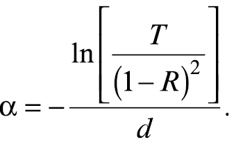 (11)
(11)
Thus with allowance for reflection Eq. (10) can be transformed as follows:
 (12)
(12)
The transmittances of the substrate and the structure and the reflectance of the structure at the film side can be measured with a spectrophotometer. Our measurement results are shown in Fig.
The thicknesses and the refractive indices of the films can be calculated using the spectrophotometric method of reflection at two angles of incidence [

(1, 3 and 5) Transmittance and (2 and 4) reflectance spectra of (3 and 4) typical structure, (1 and 2) substrate and (5) film.

Light reflection measurement data for 10 deg incidence angle on specimen taken at (1) fused quartz substrate side and (2) film side.
The reflectance spectra of the specimens (Fig.
To evaluate the refractive index of the deposited layer we used the reflectance spectra for two non-polarized light incidence angles, i.e., φ1 = 10 deg and φ2 = 20 deg.
First of all refractive indices are measured. To do this, the wavelengths λφ1 and λφ2 corresponding to the same interference extremum for each interference extremum are selected on the obtained spectra. Then the film refractive index for the narrow wavelength range λφ1 – λφ2 was determined using the formula
 (13)
(13)
where b is the coefficient determined as follows:
 (14)
(14)
The final value of the film refractive index is calculated using the following equation:
 (15)
(15)
As a result of the calculations we obtain a discrete array of refractive indices. The dispersion dependence of the refractive index is determined by approximating the calculated data using e.g. the Cauchy equation as follows:
 (16)
(16)
where A, B and C are material constants.
The optical thickness of the film (df∙nf) is determined using the following formula:
 (17)
(17)
where λ1, λ2 are the wavelengths of adjacent interference extrema in the interference response taken at one incidence angle, nm; and k is a coefficient which takes on 2 if two adjacent maxima are taken or 4 if adjacent maximum and minimum are taken.
With allowance for the film refractive index obtained using Eq. (15) the film thickness can be calculated as follows:
 (18)
(18)
The refractive index evaluation results obtained using the reflection spectrophotometric method for two incidence angles and their approximation results obtained using the Cauchy equation (Eq. (16)) are shown in Fig.

Dispersion dependence of refractive index of typical specimen: (1) data obtained by calculation using Eq. (16) and (2) Cauchy approximation.

Refractive and absorption indices with and without allowance for reflection for a typical specimen in the 450–1200 nm region
| λ (nm) | n | Α f (μm–1) | |
| With allowance for reflection | Without allowance for reflection | ||
| 450 | 2.153 | 0.603 | 0.959 |
| 500 | 2.075 | 0.367 | 0.744 |
| 550 | 2.018 | 0.192 | 0.391 |
| 600 | 1.974 | 0.222 | 0.553 |
| 650 | 1.940 | 0.157 | 0.471 |
| 700 | 1.913 | 0.191 | 0.580 |
| 750 | 1.891 | 0.057 | 0.221 |
| 800 | 1.873 | 0.160 | 0.591 |
| 850 | 1.858 | 0.161 | 0.578 |
| 900 | 1.846 | 0.054 | 0.244 |
| 950 | 1.835 | 0.041 | 0.237 |
| 1000 | 1.826 | 0.116 | 0.495 |
| 1050 | 1.818 | 0.160 | 0.629 |
| 1100 | 1.812 | 0.138 | 0.544 |
| 1150 | 1.806 | 0.075 | 0.345 |
| 1200 | 1.801 | 0.022 | 0.188 |
4. Conclusion
Ta–Si–C–N single-layer films were synthesized by magnetron sputtering on fused quartz substrates. The structural perfection of the films was studied using X-ray diffraction, scanning electron microscopy and glow discharge optical emission spectroscopy.
The 200–2500 nm transmittance spectra of the structures and the fused quartz substrates for normal light incidence and the reflectance spectra at 10 and 20 deg incidence angles were measured using multi-angle spectrophotometry.
A formula for determination of the film absorption coefficient based on the measured parameters was derived. The experimental and calculated data were used for plotting the absorption spectra of the substrate, structure and film, with and without allowance for reflection.
Using experimental methods based on the measurement of interference extrema in the reflectance spectra, the film thickness was estimated to be df. = 1046 nm ± 13 %, and discrete film refractive indices were obtained. The results were approximated using the Cauchy equation.
Acknowledgments
The studies were carried out with financial support within State Assignment FSME-2020-0031 (0718-2020-0031) at the Accredited Test Laboratory of Single Crystals and Stock on their Base of National University of Science and Technology MISiS.
References
- 1. Kondrashin V.I. Determination of SnO2 thin optically transparent films’ thickness by the envelope method. University Proceedings. Volga Region. Engineering Sciences. 2016; 38(2): 93–101. (In Russ.). https://izvuz_tn.pnzgu.ru/tn8216
- 2. Usanov D.A., Skripal Al.V., Skripal An.V., Abramov A.V., Bogolyubov A.S., Bakui A. Measurement of parameters of nanometer films by optical and radio wave methods. Izvestiya vysshikh uchebnykh zavedeniy. Elektronika = Proceedings of Universities. Electronics. 2010; 83(3(83)): 44–50. (In Russ.). https://elibrary.ru/mngzfd
- 3. Kiselev D.A., Zhukov R.N., Bykov A.S., Malinkovich M.D., Parkhomenko Yu.N., Vygovskaya E.A. Initiation of polarized state in lithium niobate thin films synthesized on isolated silicon substrates. Izvestiya vysshikh uchebnykh zavedenii. Materialy elektronnoi tekhniki = Materials of Electronics Engineering. 2012; (2): 25–29. (In Russ.). https://doi.org/10.17073/1609-3577-2012-2-25-29
- 4. Zhuravleva P.L., Shchur P.A., Melnikov A.A. Study of the structural parameters of thin films by analytical methods. Trudy VIAM. 2019; 78(6): 104–113. https://dx.doi.org/10.18577/2307-6046-2019-0-6-104-113
- 5. Shayapov V.R. An integrated approach to the determination of the physical properties of thin films. In: Third interdisciplinary youth scientific forum with international participation “New Materials”. Moscow; 2017. 386 p. (In Russ). https://elibrary.ru/xnvfyt
- 6. Brus V.V., Kovalyuk Z.D., Maryanchuk P.D. Optical properties of TiO2–MnO2 thin films fabricated by electron-beam evaporation. Zhurnal tekhnicheskoy fiziki. 2012; 82(8): 110–113. (In Russ). https://journals.ioffe.ru/articles/viewPDF/10683
- 7. Bobrovnikov Yu.A., Kozar’ A.V., Popov K.V., Tikhonov A.N., Tikhonravov A.V., Trubetskov M.K. Investigation of the inhomogeneity of thin films by spectrophotometric methods. Vestnik Moskovskogo universiteta. Seriya 3. Fizika, Astronomiya. 1997; (4): 24—27. (In Russ.). http://vmu.phys.msu.ru/file/1997/4/97-4-24.pdf
- 8. Sokolov V.I., Marusin N.V., Panchenko V.Ya., Savelyev A.G., Seminogov V.N., Khaidukov E.V. Determination of refractive index, extinction coefficient and thickness of thin films by the method of waveguide mode excitation. Kvantovaya elektronika. 2013; 43(12): 1149—1153. (In Russ.). http://www.mathnet.ru/php/archive.phtml?wshow=paper&jrnid=qe&paperid=15272&option_lang=eng
- 9. Vanyukhin K.D., Zakharchenko R.V., Kargin N.I., Seidman L.A. Peculiarity of forming transparent conducting films on basis of oxides indium-tin for contacts on GaN-based light emitting diodes. Izvestiya vysshikh uchebnykh zavedenii. Materialy elektronnoi tekhniki = Materials of Electronics Engineering. 2013; (2): 60–64. (In Russ.). https://doi.org/10.17073/1609-3577-2013-2-60-64
- 10. Abgaryan K.K., Bazhanov D.I., Mutigullin I.V. Theoretical investigation of electronic and structural properties of AlN thin films. Izvestiya vysshikh uchebnykh zavedenii. Materialy elektronnoi tekhniki = Materials of Electronics Engineering. 2015; 18(1): 48–51. (In Russ.). https://doi.org/10.17073/1609-3577-2015-1-48-51
- 11. Khomchenko A.V., Sotsky A.B., Romanenko A.A., Glazunov E.V., Shulga A.V. Waveguide method for measuring the parameters of thin films. Zhurnal tekhnicheskoy fiziki. 2005; 75(6): 98–106. (In Russ.). https://journals.ioffe.ru/articles/viewPDF/8584
- 12. Sakhbiev T.R. Two-frequency methods for determining the thickness and dielectric parameters of thin films. Novoye slovo v nauke: perspektivy razvitiya. 2015; 4(6): 171–172. (In Russ.). https://elibrary.ru/xxxsbv
- 13. Tikhonravov A.V., Trubetskov M.K., Amotchkina T.V., DeBell G., Pervak V., Krasilnikova-Sytchkova A., Grilli M.L., Ristau D. Optical parameters of oxide films typically used in optical coating production. Applied Optics. 2011; 50(9): C75–C85. https://doi.org/10.1364/AO.50.000C75
- 14. Tikhonravov A.V., Amotchkina T.V., Trubetskov M.K., Francis R.J., Janicki V., Sancho-Parramon J., Zorc H., Pervak V. Optical characterization and reverse engineering based on multiangle spectroscopy. Applied Optics. 2012; 51(2): 245—254. https://doi.org/10.1364/AO.51.000245
- 15. Ayupov B.M., Zarubin I.A., Labusov V.A., Sulyaeva V.S., Shayapov V.R. Searching for the starting approximation when solving inverse problems in ellipsometry and spectrophotometry. Journal of Optical Technology. 2011; 78(6): 350–354. https://doi.org/10.1364/jot.78.000350
- 16. Shmidt V. Optical spectroscopy for chemists and biologists. Moscow: Tekhnosfera; 2007. 362 p. (In Russ.)
- 17. Klark E.R., Eberkhardt K.N. Microscopic methods for studying materials. Moscow: Tekhnosfera; 2007. 376 p. (In Russ.)
- 18. Bokker U. Spectroscopy. Moscow: Tekhnosfera; 2009. 528 p. (In Russ.)
- 19. Landsberg G.S. Optics: textbook for universities. Moscow: Fizmalit; 2006. 848 p. (In Russ.)
- 20. Konstantinova A.F., Grechushnikov B.N., Bokut B.V., Valyashko E.G. Optical properties of crystals. Minsk: Navuka i tekhnika; 1995. 303 p. (In Russ.)
- 21. Tolmachev G.N., Kovtun A.P., Pavlenko A.V., Zakharchenko I.N., Aliev I.M., Reznichenko L.A., Verbenko I.A. Synthesis, structure, and optical characteristics of barium-strontium niobate thin films. Physics of the Solid State. 2015; 57(10): 2106–2111. https://doi.org/10.1134/S1063783415100339
- 22. Ayupov B.M., Rumyantsev Yu.M., Shayapov V.R. Particular features of determination of the thickness of dielectric films obtained in researches. Poverkhnost’. rentgenovskiye, sinkhrotronnyye i neytronnyye issledovaniy. 2010; (5): 100–105. (In Russ.). https://elibrary.ru/msqeaj
- 23. Manifacier J.C., Gasiot J., Fillard J.P. А simple method for the determination of the optical constants n, h and the thickness of a weakly absorbing thin film. Journal of Physics E: Scientific Instruments. 1976; 9(11): 1002–1004. https://doi.org/10.1088/0022-3735/9/11/032
- 24. Swanepoel R. Determination of the thickness and optical constants of amorphous silicon. Journal of Physics E: Scientific Instruments. 1983; 16(12): 1214–1223. https://doi.org/10.1088/0022-3735/16/12/023
- 25. Kiryukhantsev-Korneev Ph.V., Sytchenko A.D., Sviridov T.A., Sidorenko D.A., Andreev N.V., Klechkovskay V.V., Polčak J., Levashov E.A. Effects of doping with Zr and Hf on the structure and properties of Mo-Si-B coatings obtained by magnetron sputtering of composite targets. Surface and Coatings Technology. 2022: 128141. https://doi.org/10.1016/j.surfcoat.2022.128141
- 26. Born M., Vol’f E. Fundamentals of optics. Moscow: Nauka; 1970. 855 p. (In Russ.)
- 27. Karamaliyev R.A., Qajar C.O. Optical properties of composite thin films containing silver nanoparticles. Journal of Applied Spectroscopy. 2012; 79(3): 404–409. https://doi.org/10.1007/s10812-012-9615-1
- 28. Shalimova K.V. Physics of semiconductors. Moscow: Energiya; 1971. 400 p. (In Russ.)
- 29. Efimov A.M. Optical properties of materials and mechanisms of their formation: textbook. Saint Petersburg: SPbGUITMO; 2008. 103 p. (In Russ.)
- 30. Bohren C.F., Huffman D.R. Absorption and scattering of light by small particles. John Wiley & Sons, Inc.; 1983. 545 p.