|
Corresponding author: Arkady V. Naumov ( naumov_arkadii@mail.ru ) © 2020 Nikolay A. Kulchitsky, Arkady V. Naumov, Vadim V. Startsev.
This is an open access article distributed under the terms of the Creative Commons Attribution License (CC BY 4.0), which permits unrestricted use, distribution, and reproduction in any medium, provided the original author and source are credited.
Citation:
Kulchitskiy NA, Naumov AV, Startsev VV (2020) Photonic and Terahertz applications as the next gallium arsenide market driver. Modern Electronic Materials 6(3): 77-84. https://doi.org/10.3897/j.moem.6.3.63224
|
Abstract
Analysis of current GaAs and related device market initiated in a number of earlier works has been continued. Binary semiconductor GaAs compound is a conventional MW electronics material. Until recently GaAs based HF ICs for mobile phones were among the most rapidly growing segments of GaAs market. However the GaAs market development trend is changing. Photonics and Terahertz engineering are becoming the new world GaAs market drivers. This means that the current emphasize of GaAs single crystal technologies will shift toward vertical directional crystallization of “optoelectronic quality” crystals. In the medium and longer terms the world GaAs wafer and epitaxial structure markets will continue growing. In the shorter term we all will have to take into account COVID epidemic consequences. Still the GaAs market is closely related to Smartphone market novelties. Quite probably after a long growth period the GaAs market will keep on shrinking for the second consecutive year: GaAs production may decline by 11–12% in 2020. Assuming that the epidemic will be somehow taken under control in 2021 the overall Smartphone production can probably be expected to grow starting from 2021.
Currently the Russian market of semiconductor compounds for photonics and electronic components (GaAs etc.) is but moderate and in predictable terms is not expected to achieve a level that is required for the emergence of a competitive domestic manufacturer, even though all importation replacement programs are accomplished. Meanwhile there is understanding that developing an advanced electronic components industry in Russia requires larger production of source materials.
Keywords
gallium arsenide, Czochralski method, vertical directional crystallization, epitaxial GaAs wafers, market, prices, demand, consumption
1. Introduction
This work is a continuation of an earlier one [
2. Gallium arsenide (GaAs): new outlooks
In the mid 1960s US and USSR started investigating properties of GaAs single crystals, eventually coming to the development of high performance integrated circuits (IC) used in smart weapon control systems and supercomputers. The cost of RF transistors reduced considerably in the 2010s upon the industrial implementation of 150 mm GaAs wafer processing technologies. This has enabled their widespread use in every application domain, from mobile phones and base stations to radars and mm range communication systems. In 2019 RF applications reached 33% of GaAs markets by size and 37% by price. GaAs is also widely used in optoelectronics as a basic material for LEDs. It seems however that the current GaAs market development trend is changing from RF-electronics to photonics. The threshold seems to be the year 2017 when iPhoneX Smartphones received a 3D scanning function with GaAs based vertical cavity surface emitting lasers (VCSEL). Another quite important milestone is the emergence of a GaAs based quantum well staring focal plane array market. THz range devices including GaAs based ones acquire increasing importance in various applications (e.g. security, medicine and image rendering) [
The world market of GaAs devices was $10 bn in 2019 and will exceed $15 bn in 2027 (Fig.
| Devices | Structure | Application | GaAs wafer technology type |
|---|---|---|---|
| Visible range LEDs incl. micro-LEDs | GaAlAs, GaAsP or InGaAsP epitaxial layers on GaAs wafers | Standard luminance LEDs for indicators, digital displays and IR emitters; high luminance LEDs for backlighting, illumination, alarm devices, nameplates, car lights etc. | VGF |
| LEDs incl. VCSEL, EEL,IR, UV etc. | GaAlAs, GaAsP etc. epitaxial layers on GaAs wafers | CD and DVD read/write units, telecommunication devices, FOCL, medicine, printers, solid state laser excitation, LiDAR optical detection | VGF |
| Solar cells | doped GaInAs or AlGaInP epitaxial layers on Ge | Space vehicle onboard power units; growing markets of ground batteries of this type | VGF, LEC |
| Analog and digital ICs | GaInP, GaInAs, AlGaInP etc. epitaxial layers on GaAs wafers | High performance logic units, communication units for telecommunication systems, mobile phone power amplifiers | LEC |
| IR array photocell devices, THz generators and detectors | GaInAs etc. epitaxial structures and quantum well structures on GaAs wafers | Infrared night vision devices and THz range detectors | VGF |

3. GaAs single crystal growth: specific features
As noted earlier [
- Semiinsulating (SI) GaAs with a high specific resistivity / intrinsic conductivity (10 7 Ohm×cm). Used in HF ICs and discrete microelectronic devices.
- Doped (SC)n-conductivity GaAs with a low dislocation density. Single crystals of highly doped (10 17–10 18 cm -3) GaAs along with a high conductivity should have a highly perfect crystal structure. They are used in optoelectronics for injection lasers, LEDs and photodiodes, photosensitive cathodes, MW and THz generators.
Industrial GaAs single crystals are grown using three fundamental methods: Liquid Encapsulated Czochralski (LEC), horizontal directional (Horizontal Bridgman (HB) or Horizontal Gradient Freeze (HGF)) and vertical directional (Vertical Bridgman (VB) or Vertical Gradient Freeze (VGF)).
An important feature of LEC is that the single crystal is grown in high axial and radial temperature gradients near the crystallization front, i.e., where the plasticity of the material is the highest. Crystal growth in high temperature gradients by LEC entails a high dislocation density. Typical ND of undoped LEC single crystals may be as high as (1–2) × 105 cm-2 for 100–200 mm diam. ingots. LEC materials have more homogeneous specific resistivity distribution in wafer section.
VGF materials have a lower dislocation density. Unlike MW devices, dislocations are detrimental in active zones of light emitting structures as they cause fast device performance degradation. Therefore the low dislocation density ND requirement is the basic one for highly doped wafer materials. There is the following commonly used classification: LED fabrication requires crystals with ND < 5 × 10³–1 × 104 cm-2, while for laser fabrication crystals with ND < 5 × 102 cm-2 are needed.
Unlike MW ICs, the greatest device cost contribution in optoelectronic device processes comes from operations downstream of structure chipping. Therefore growing larger diameter wafers is not of crucial importance for optoelectronic device technologies. As a result LED and laser technologies still consume lots of <100 mm wafers although the industry can already deliver low dislocation density single crystals as large as 200 mm in diameter.
Both LEC and VGF methods can provide SC and SI GaAs single crystals. Importantly, VGF grown single crystals are more expensive than LEC ones, owing to 4–5 times lower crystallization rates and no reseeding operation. Comparing the totality of the parameters for different growth methods one can see that for most MW applications, it is preferred (at least economically) to use LEC GaAs whereas VGF GaAs is indispensable for LED and all optoelectronic applications (Table
IR modules of some manufacturers with cooled GaAs quantum well photodetectors
 |
 |
 |
 |
|
|---|---|---|---|---|
| Photodetector Model | IRnova320ER-LW IDCA | Irnova640 integral cooler DDCA | Irnova640-ER split cooler DDCA | ASTROHN-640KYa20A89 |
| Photodetector Array Format | 320 × 256 | 640 × 480 | 640 × 512 | 640 × 512 |
| Array Step, μm | 30 | 25 | 25 | 20 |
| Spectral Range, mm | 7.5–9.0 | 7.5–9.0 | 7.5–9.0 | 8.3–8.7 |
| Maximum Spectral Sensitivity, mm | 8.6 | 8.6 | 8.6 | 8.7 |
| Time NETD, mK | 25 | 35 | 30 | 30 |
| Frame Rate, Hz | 60 | 30 | 107 | 50 |
| Cooling System | Integral Stirling | Integral Stirling | Split Stirling | ASTROHN-MKS500 Integral Stirling |

4. GaAs epitaxy
GaAs devices are fabricated by metal-organic chemical vapor deposition (MOCVD) epitaxy or molecular beam epitaxy (MBE) on GaAs wafers (Fig.

Major manufacturers of (a) GaAs ingots and wafers [5] and (b) epitaxial GaAs structures [6].


5. New optoelectronic GaAs applications
5.1. Laser diodes (VCSEL etc.)
Apple’s iPhoneX Smartphone was the first mass consumer device to use the face recognition technology where an IR photosensor scans user’s face to build a 3D model. In iPhoneX 150-mm GaAs wafers are used for the fabrication of face recognition VCSELs and photodetectors, and this market will keep on growing (Fig.
LiDAR (Light Identification Detection and Ranging) technology for retrieving and processing information on remote objects with the aid of active optical systems is the key technology that allows creating a 3D map of surrounding areas for unmanned vehicles and in a wide range of robotics applications. This new application uses high power large size GaAs edge emission laser (EEL) devices which are expected to give a strong impetus to the growth of “photonic” GaAs wafer markets (Fig.
Expectably the segment of infrared LEDs on GaAs wafers will also exhibit a dynamic growth until 2025. GaAs infrared LEDs, used in medical blood pressure and blood sugar sensors and in gesture recognition sensors of Smartphones and cars, are still another important segment of the growing GaAs market [
Hereinafter while analyzing GaAs application fields we will for clarity classify conventional visible range LEDs as the “LED” category, and VCSEL, EEL, IR etc. LEDs, as the “optoelectronics” category.
5.2. Quantum well photodetector heat vision devices
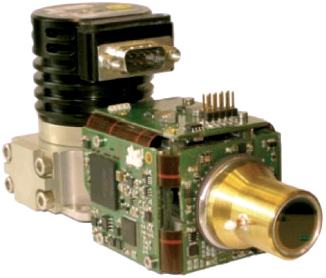
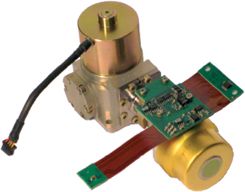
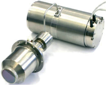
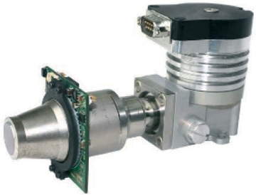
The growing demand for IR systems for military and civilian applications will entail expansion of the worldwide thermal vision camera market in the next few years. The thermal vision camera market for military and security applications is predicted by analysts to exceed $2.4 bn by 2023 due to aggravation of security problems. The significant expansion of short-wave range (0.9–1.7 mm) IR systems has also entailed the emergence of cooled array quantum well photodetector devices (QWIP) (Fig.
Table
5.3. THz optoelectronics
The THz radiation region of electromagnetic radiation lies between the infrared and the millimeter regions. Different sources provide different treatise of the boundaries between these radiation types. For definitiveness, we will accept that the THz region is within 0.1–10 THz (30–3000 mm) partially overlapping with the middle infrared (2.5–50 mm) and the millimeter (30–300 THz, 1–10 mm) regions and includes narrower submillimeter and sub-THz regions. Devices working in the THz region find increasing applications (e.g. in security, medicine, astrophysics etc.).
Although the THz technologies have been developing quite rapidly in recent years the fabrication of highly sensitive compact detectors and THz radiation generators is still a complex research task. The development of THz technologies is complicated for their working ranges are between the conventional radio frequencies and the optical electromagnetic spectrum region. Detection of THz radiation does not obey some fundamentals of photon and electronic device operation. THz radiation has typically low photon energies (4 meV for 1 THz radiation) and hence photon THz devices with quantum transitions are suitable for low-temperature operation only. The maximum operation frequency of electronic devices is determined by the electron path time in the device active region which in turn depends on carrier velocity. For GaAs heterostructures the maximum electron velocity in the active region is on the order of a few 107 cm/s whereas the plasma wave velocity in the transistor sub-gate channel is two orders of magnitude higher. This fact has allowed the development of GaAs THz radiation detectors.
5.3.1. GaAs Shottky barrier THz detectors
Shottky barrier structures are among the main THz technology components. Shottky diodes are considerably faster than conventional p-n junction diodes, and this allows their use at frequencies of up to several THz. This property of Shottky diodes is accounted for by the fact that charge transport in these devices occurs mainly by thermal emission of electrons via the energy barrier at the metal/semiconductor contact. These receivers are typically designed with Shottky diode beam contacts integrated in antennas. Epitaxial GaAs is the most frequently used semiconductor for planar Shottky diode mixers [
5.3.2. GaAs FET transistor THz detectors
Another widely used category of THz radiation detectors are high electron mobility GaAs field effect transistor (FET) detectors. The source and drain of these transistors are interconnected by a planar channel filled with 2D electron gas in which THz frequency plasma waves may propagate. The nonlinear properties of plasma excitations (electron density waves) in nanosized FETs provide their response at far higher frequencies than the device threshold frequency due to ballistic electron transport. These receivers may be operated over a wide temperature range, up to room temperature [
5.3.3. Quantum well THz detectors
The possibility of THz radiation detection by GaAs structure quantum well receivers is based on the use of inter-subband transitions in periodical GaAs QW-structures, i.e., superlattices. These structures can be used as wide-band THz detectors.
Currently THz device market is at an early development stage, so one can hardly predict which share of GaAs products will be consumed by THz applications. It is however undisputed that it will become quite big in the medium term.
6. GaAs market development until 2025
Analysts predict about 10% annual growth of the entire GaAs wafer market until 2025. In financial terms the GaAs wafer market will grow from $200 mln in 2019 to $349 mln in 2025 [

7. GaAs manufacturers worldwide and in Russia and existing business models
The major manufacturers of GaAs products (ingots, wafers and epitaxial layers) are Freiberger Compound Materials, AXT, Sumitomo Electric, China Crystal Technologies, Shenzhou Crystal Technology, Tianjin Jingming Electronic Materials, DOWA Electronics Materials, II–VI Incorporated, IQE Corporation and Wafer Technology. Sumitomo Electric, Freiberger Composite Materials and AXT lead the market of large-size GaAs crystals with an approx. 95% total share.
Currently GaAs crystals in Russia are grown by Giredmet JSC (Moscow, Rosatom Enterprise, LEC method) and by Lassard Ltd. (Obninsk, VGF method). Giredmet JSC and Lassard Ltd. have launched investment projects for GaAs technology development. Furthermore, GaAs heterostructure fabrication was started in 2019. JSC Ekran-Optical Systems started an MBE plant based on developments of the A.V. Rzhanov Institute of Semiconductor Physics, Siberian Branch of RAS (ISP) [
Since new applications (laser and THz) impose extremely high and ever growing technical requirements to GaAs wafers, analysts believe that the VGF method will be dominating in this segment and the abovementioned market players will retain their technical advantage for at least 3–5 years ahead. It is expected that Chinese GaAs wafer suppliers like Violent Materials which have occupied part of LED market that was formerly controlled by leading suppliers will further increase their market share [
Different business models exist for the fabrication of GaAs epitaxial structures and GaAs devices (Fig.

8. Conclusion
Photonic applications are becoming the main GaAs market driver. In the medium and longer terms the world GaAs wafer and epitaxial structure markets will continue growing.
In the shorter term we all will have to take into account COVID epidemic consequences. This is important for assessing GaAs production since the GaAs market is closely related to Smartphone market novelties. Smartphone production for 2020 was predicted at a 1.24 bn pcs level, i.e., 11.3% y/y market shrinkage [
Currently the Russian market of semiconductor compounds for photonics and electronic components (GaAs etc.) is but moderate and in predictable terms is not expected to achieve a level that is required for the emergence of a competitive domestic manufacturer, even though all import replacement programs are accomplished. Meanwhile there is understanding that developing an advanced electronic components industry in Russia requires larger production of source materials.
Regarding recommendable GaAs market development trends for Russia which should be given the main effort, one should pay primary attention to the development of VGF technologies for low-dislocation GaAs single crystals and wafers for epitaxy.
References
- 1 Majanov E.P., Kniazev S.N., Naumov A.V. GaAs single crystals market: development trends. Izvestiya Vysshikh Uchebnykh Zavedenii. Materialy Elektronnoi Tekhniki = Materials of Electronics Engineering, 2016; 19(3): 156–162. (In Russ). https://doi.org/10.17073/1609-3577-2016-3-156-162
- 2 Markov A.V. Single crystals of semiconductor compounds III–V: modern production and prospects for its development. Izvestiya vuzov. Fizika, 2003; (6): 5–11. (In Russ.)
- 3 Kulchitsky N.A., Naumov A.V., Startsev V.V. New trends in the development of the gallium arsenide devices market. Adv. Appl. Phys., 2020; 8(2): 136–147. (In Russ.)
- 4 Khludkov S.S., Tolbanov O.P., Vilisova M.D., Prudaev I.A. Poluprovodnikovye pribory na osnove arsenida galliya s glubokimi primesnymi tsentrami [Semiconductor devices based on gallium arsenide with deep impurity centers]. Tomsk: Izdatel’skii Dom Tomskogo gosudarstvennogo universiteta, 2016: 145. (In Russ.)
- 5 Kishchinskii A.V. Broadband transistor amplifiers of the microwave range: the generation change. Elektronika: nauka, tekhnologiya, biznes, 2010; (2): 5–10. (In Russ.)
- 6 GaAs wafer market growing at 15% CAGR to 2023, driven by photonics applications growing at 37%. URL: www.semiconductor-today.com/news_items/2018/jul/yole_240718.shtml (accessed: 23.10.2020)
- 7 GaAs Wafer & Epiwafer Market: RF, Photonics, LED и PV приложения. URL: https://www.i-micronews.com/products/gaas-wafer-and-epiwafer-market-rf-photonics-led-and-pv-applications/?cn-reloaded=1 (accessed: 23.10.2020)
- 8 Dietrich C.P., Fiore A., Thompson M.G., Kamp M., Höfling S. GaAs integrated quantum photonics: Towards compact and multi-functional quantum photonic integrated circuits. Laser Photonics Rev., 2016; 10(6): 870–894. https://doi.org/10.1002/lpor.201500321
- 9 GaAs Market Overview. URL: https://anysilicon.com/gaas-market-overview-apple-changing-future/ (accessed: 23.10.2020)
- 10 Apple Is Changing GaAs Future. URL: https://compoundsemiconductor.net/article/104852/Apple_Is_Changing_GaAs_Future (accessed: 23.10.2020)
- 11 Yoon J., Jo S., Chun I. S., Jung I., Kim H.-S., Meitl M., Menard E., Li X., Coleman J. J., Paik U., Rogers J. A. GaAs photovoltaics and optoelectronics using releasable multilayer epitaxial assemblies. Nature, 2010; 465: 329–333. https://doi.org/10.1038/nature09054
- 12 How Will COVID-19 Affect GaAs Revenue. URL: https://www.strategyanalytics.com/strategy-analytics/blogs/components/advanced-semiconductors/advanced-semiconductors/2020/05/04/how-will-covid-19-affect-gaas-revenue?slid=1066895&spg=8 (accessed: 23.10.2020)
- 13 GaAs wafer market growing at 10% CAGR to more than $348m by 2025. Semiconductor Today. Compounds & Advanced Silicon, 2020; 15(5): 56–57. URL: http://www.semiconductor-today.com/news_items/2020/jun/yole-020620.shtml
- 14 Sizov F. THz radiation sensors. Opto-Electronics Rev., 2010; 18(1): 10–36. https://doi.org/10.2478/s11772-009-0029-4
- 15 Sizov F., Rogalski A. THz detectors. Progress in Quantum Electronics, 2010; 34(5): 278–347. https://doi.org/10.1016/j.pquantelec.2010.06.002
- 16 Stafeev V. I. Telluridy kadmiya-rtuti: fotopriemniki infrakrasnoao diapazona, drugie pribory [Cadmium-mercury tellurides: infrared photodetectors, other devices]. Moscow: FGUP «NPO “Orion”», 2011: 204. (In Russ.)
- 17 JSC “Screen-optical systems” launched the first industrial production of nanoheterostructures based on gallium arsenide in Russia. URL: http://www.ratm.ru/press-center/news/ao-ekran-opticheskie-sistemy-zapustilo-pervoe-v-rossii-promproizvodstvo-nanogeterostruktur-na-osnove/ (accessed: 23.10.2020). (In Russ.)
- 18 Novosibirsk scientists have made a prototype installation for growing semiconductors in space. URL: https://infopro54.ru/news/novosibirskie-uchenye-izgotovili-opytnyj-obrazec-ustanovki-dlya-vyrashhivaniya-poluprovodnikov-v-kosmose/?utm_source=yxnews&utm_medium=desktop (accessed: 23.10.2020). (In Russ.)
- 19 Smartphone production falls a record 16.7% year-on-year in Q2/2020. Semiconductor Today. Compounds & Advanced Silicon, 2020; 15(7): 76–77. URL: http://www.semiconductor-today.com/news_items/2020/aug/trendforce-260820.shtml