|
||
|
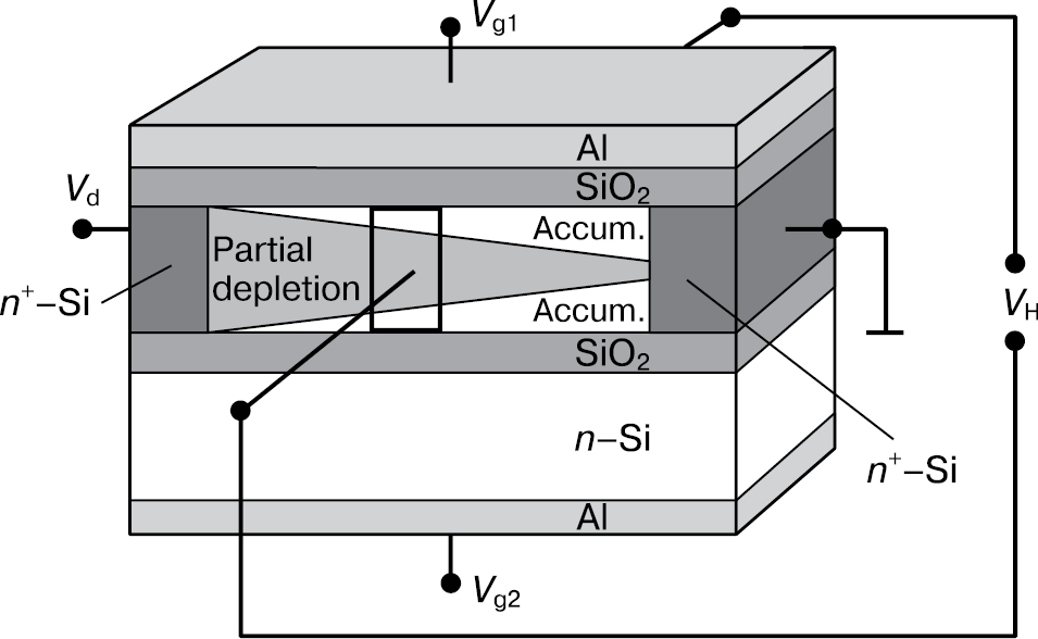
FHS schematic and working principle explanation: Vd is the FHS power voltage, Vg1 and Vg2 are the top and bottom FHS gate bias, respectively, and VH is the Hall voltage read at the Hall probes. |
|
||||||||
| Part of: Leonov AV, Murashev VN, Ivanov DN, Kirilov VD (2020) Coupling effect in field Hall elements based on thin-film SOI MOS transistors. Modern Electronic Materials 6(4): 155-158. https://doi.org/10.3897/j.moem.6.4.65567 |