|
||
|
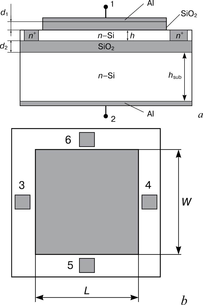
Dimensions and arrangement of SOI FHS elements: (a) cross-section and (b) top view; (1 and 2) top and bottom gate contacts; (3 and 4) current (Ohmic) contacts and (5 and 6) side Hall probes. Parameters: h = 0.2 µm is the working silicon layer thickness, d1 = 0.35 µm is the top gate dielectric thickness, d2 = 0.35 µm is the SOI structure buried dielectric layer thickness, hsub = 400 µm is the substrate thickness, L = 500 µm is the silicon channel length and W = 500 µm is the silicon channel width |