|
||
|
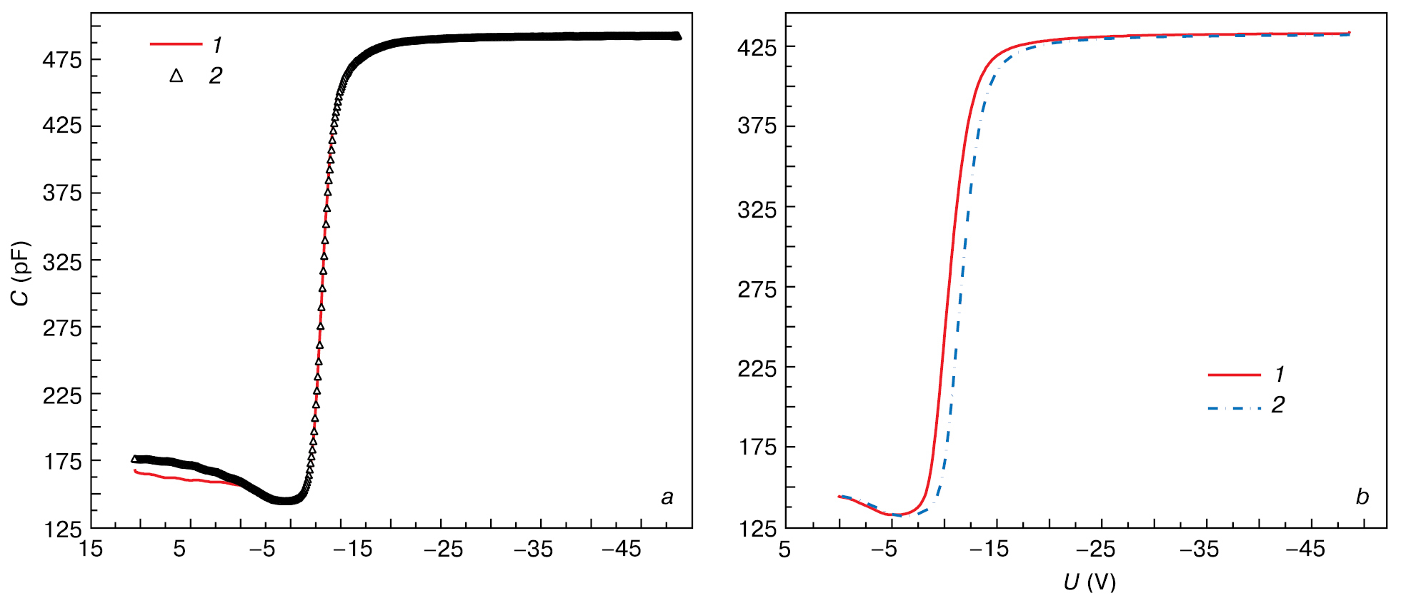
Variation of C–V curves of test MOS structure before electron beam irradiation for application of different bias to metallization (a) +40 V (inversion), (b) –40 V (accumulation), (1) before biasing and (2) after biasing for 15 min. |
|
||||||||
| Part of: Kulanchikov YO, Vergeles PS, Yakimov EB (2019) Effect of low-energy electron irradiation on voltage-capacity curves of Al/SiO2/Si structure. Modern Electronic Materials 5(4): 175-179. https://doi.org/10.3897/j.moem.5.4.52311 |