|
||
|
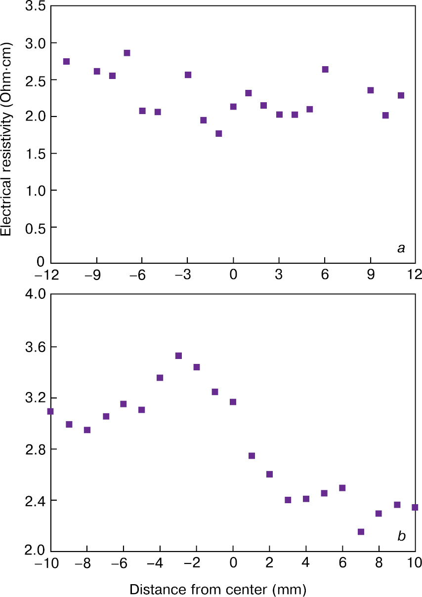
Contactless technique electrical resistivity distribution along quadrate diagonal for textured specimens with (a) 10 min and (b) 15 min etched porous silicon layer. |
|
||||||||
| Part of: Latukhina NV, Kobeleva SP, Rogozhina GA, Shishkin IA, Schemerov IV (2018) Contact and contactless porous silicon parameter measurement techniques. Modern Electronic Materials 4(4): 143-150. https://doi.org/10.3897/j.moem.4.4.39503 |